

Semiconductor device and manufacturing method thereof
a technology of semiconductor devices and semiconductors, applied in semiconductor devices, semiconductor/solid-state device details, electrical apparatus, etc., can solve problems such as difficulty in achieving the target accuracy of high-speed oco circuits, and achieve the effect of free from resistance variations
- Summary
- Abstract
- Description
- Claims
- Application Information
AI Technical Summary
Benefits of technology
Problems solved by technology
Method used
Image

Examples
embodiment 1
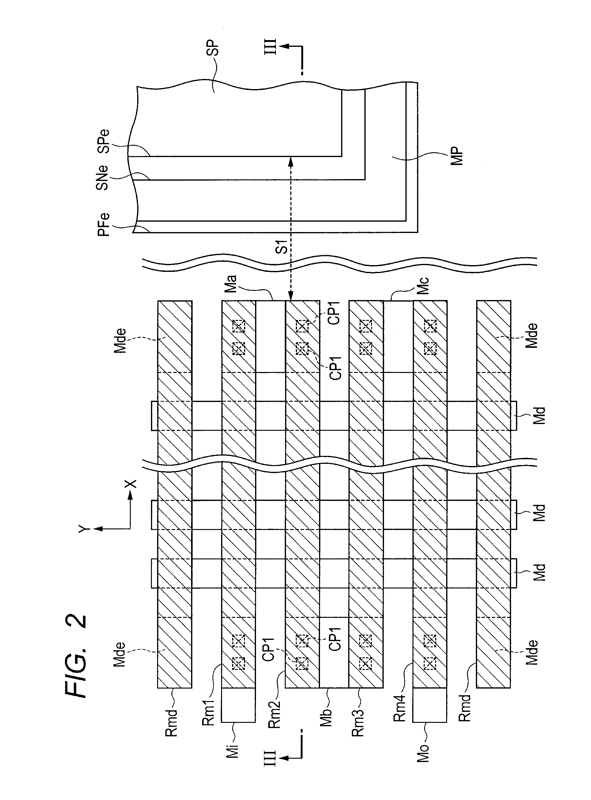
[0057]Referring to FIGS. 2 and 3, a partial structure of a high-speed OCO circuit will next be described as one example of a semiconductor device. FIG. 3 illustrates the cross-section taken in the direction of arrows along the line III-III in FIG. 2.
[0058]As illustrated in FIG. 3, this semiconductor device has a first interlayer insulating film SO11 provided above a substrate SUB and a plurality of dummy layers Md provided over the first interlayer insulating film SO11, arranged to have a predetermined space between any adjacent two of the dummy layers in a first direction (direction X in FIG. 2), and extending in a second direction (direction Y in FIG. 2) perpendicular to the first direction (direction X).
[0059]The first interlayer insulating film SO11 has thereover tap layers Ma and Mb placed at positions sandwiching therewith the dummy layers Md from both sides thereof in the first direction (direction X) with a predetermined space in the second direction (direction Y). In the pl...
embodiment 2
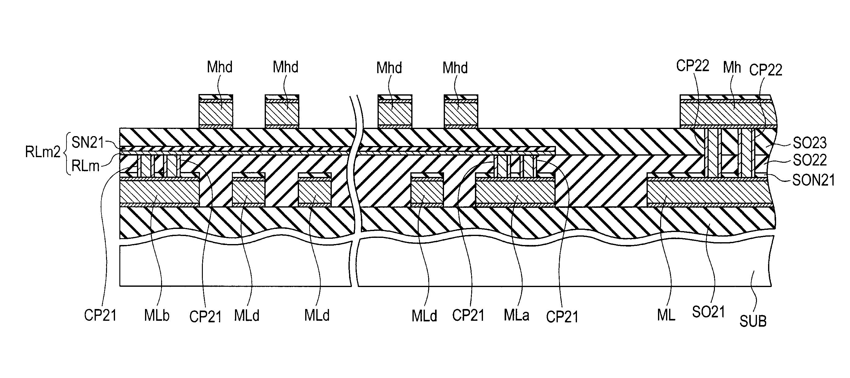
[0112]Next, referring to FIGS. 16 and 17, a partial structure of a high-speed OCO circuit will be described as one example of a semiconductor device. The entire structure of a microcomputer chip is similar to that of FIG. 1. FIG. 17 is a cross-section taken in the direction of arrows along the line XVII-XVII in FIG. 16.
[0113]As illustrated in FIG. 17, this semiconductor device has a first interlayer insulating film SO21 provided over a substrate SUB and a plurality of first dummy layers MLd provided over the first interlayer insulating film SO21, arranged to have a predetermined space between any adjacent two of the first dummy layers in a first direction (direction X in FIG. 17), and extending in a second direction (direction Y in FIG. 16) perpendicular to the first direction (direction X).
[0114]The first interlayer insulating film SO21 has thereover tap layers MLa and MLb provided with a predetermined space in the second direction (direction Y) at a position sandwiching the plural...
embodiment 3
[0147]In the next place, referring to FIGS. 30 and 31, a partial structure of a high-speed OCO circuit will be described as one example of a semiconductor device. The entire structure of the microcomputer chip is the same as that of FIG. 1. FIG. 31 illustrates the cross-section taken in the direction of arrows along the XXXI-XXXI line in FIG. 30.
[0148]As illustrated in FIG. 31, this semiconductor device has a first interlayer insulating film SO21 provided above a substrate SUB and a plurality of first dummy layers MLd provided above the first interlayer insulating film SO21, arranged to have a predetermined space between any two adjacent layers thereof in a first direction (direction X in FIG. 30), and extending in a second direction (direction Y in FIG. 30) perpendicular to the first direction (direction X).
[0149]The first interlayer insulating film SO21 has thereover a lower-level interconnect layer ML formed in the same step as that of forming the first dummy layers MLd.
[0150]The...
PUM
 Abstract
Description
Claims
Application Information