Semiconductor device and method of manufacturing same

a semiconductor and device technology, applied in semiconductor devices, semiconductor/solid-state device details, electrical apparatus, etc., can solve the problems of lithography deviation, and the insufficient contact performance of the base contact region, so as to reduce the variation in forward voltage vf and on resistance ron. the effect of stabilizing and reducing the variation of forward voltage v

Active Publication Date: 2019-05-09
FUJI ELECTRIC CO LTD
View PDF5 Cites 3 Cited by
  • Summary
  • Abstract
  • Description
  • Claims
  • Application Information

AI Technical Summary

Benefits of technology

[0017]The present invention makes it possible to provide a semiconductor device that is capable of stabilizing and reducing variation in forward voltage Vf and ON resistance Ron even if a reading error of an alignment mark occurs, and a method of manufacturing such semiconductor device.

Problems solved by technology

If different alignment marks are selected in consecutive photolithography processes, there is a risk that a positional deviation (a so-called “lithography deviation”) could occur among the semiconductor layers to be fabricated.
In particular, if the source region and base contact region undergo ion implantation with approximately the same impurity density, then in the region where the implanted ions overlap, the contact performance of the base contact region will cease to be sufficient.
Due to this, the contact resistance increases, and the ON resistance Ron and forward voltage Vf of the body diode increases, which results in defects, i.e., variation in forward voltage Vf and ON resistance Ron.
However, the number of photolithography processes would increase in order to form the large number of alignment marks, thus increasing manufacturing burdens.
However, the reading devices in already-existing manufacturing facilities are overwhelmingly a type that images the position of the alignment mark from the top surface side of the semiconductor substrate, and thus, in the case of a method that additionally installs a separate reading device, new capital investment would be needed, thus increasing costs.

Method used


Image

  • Semiconductor device and method of manufacturing same
  • Semiconductor device and method of manufacturing same
  • Semiconductor device and method of manufacturing same

Examples


embodiment 2

Structure of Semiconductor Device

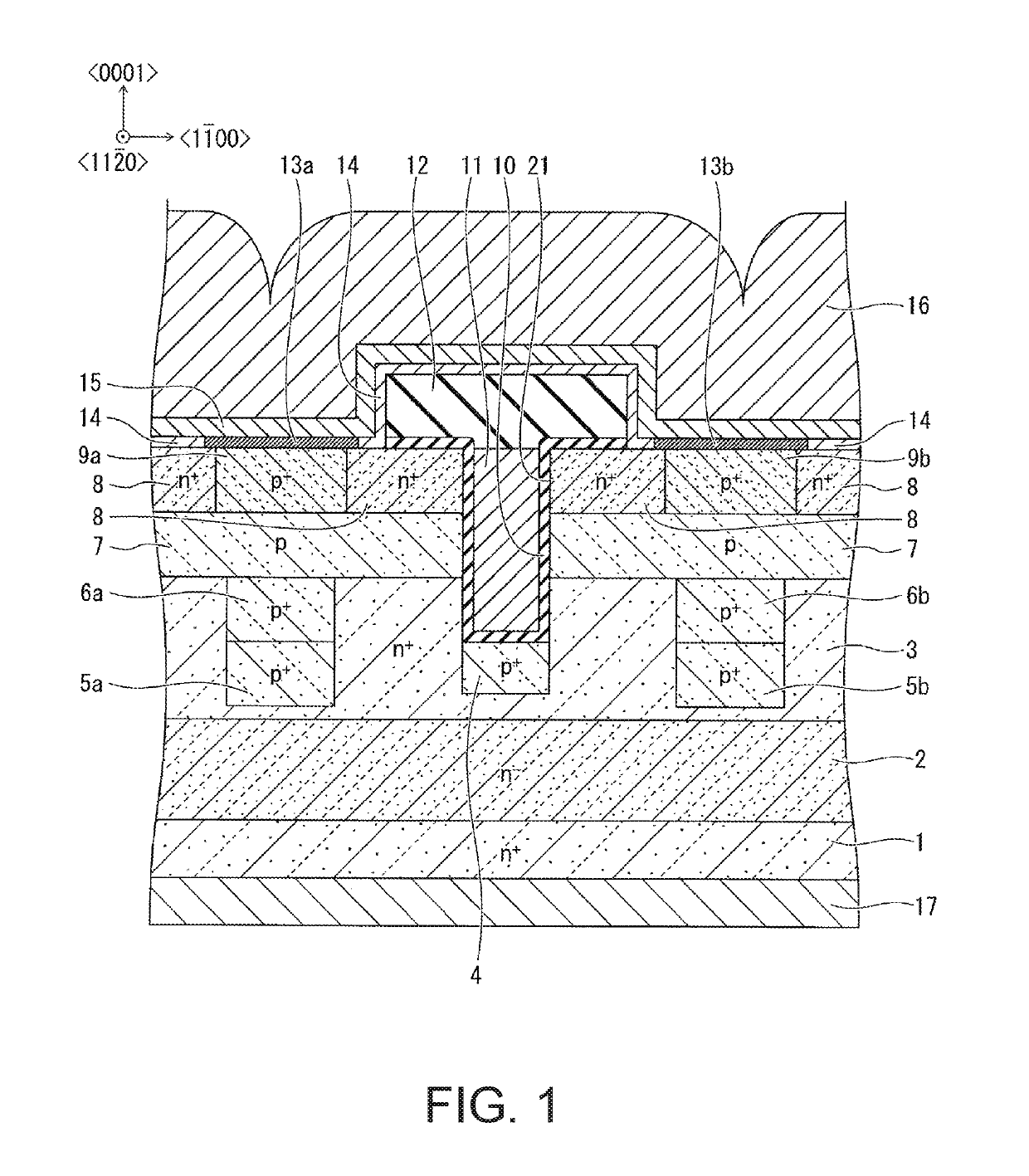
[0107]As shown in FIG. 24, the semiconductor device according to Embodiment 2 has a first gap provided on end on the bottom side of the base contact region 9a in the direction. Furthermore, a non-contact region 50 is further provided on the side opposite to the first gap, which is the top side of the base contact region 9a in the direction. The non-contact region 50 has a lower impurity density than both the base contact region 9a and source region 8. The base contact region 9a has a width wp in the direction, and the non-contact region 50 has a width wa in the direction. The width of the non-contact region 50 in the direction is approximately the same as the width of the base contact region 9a. As shown in FIG. 25, the top surface of the base region 7 is exposed at the first gap.

[0108]As shown in FIG. 26, the impurity density of the source region 8 in SiC and the impurity density of the base contact region 9a are approximately the same or close...

modification example

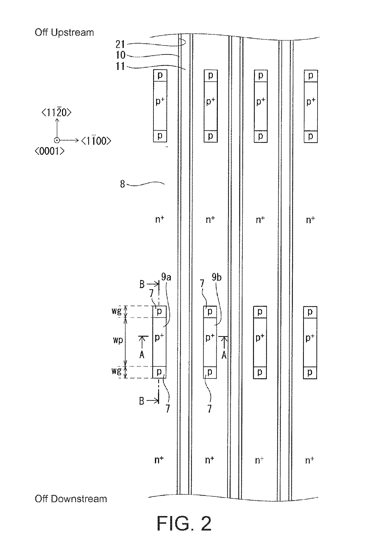
[0116]As shown in FIG. 31, the present embodiment is provided with second gaps along the direction in addition to the first gaps along the direction. FIG. 31 illustratively shows, in addition to the first gaps described in Embodiment 1, second gaps having a width wgy provided between the base contact region 9a and source region 8 along the direction. The second gaps are provided to both the left and right of the base contact regions 9a, 9b in FIG. 31.

[0117]In a similar manner to the first gaps, the second gaps formed along the direction absorb a positional deviation width Δx in the direction of the alignment mark caused by the off-angle θ and epitaxial growth and a fluctuation width in the direction caused by the positioning device. Providing the second gaps also makes it possible to reduce overlapping of the base contact region 9a and source region 8 in the direction. FIG. 31 illustratively shows a case where the second gaps along the direction are combined with the configu...


PUM


Abstract

This semiconductor device includes: an n-type SiC drift layer; a p-type base region; an n-type source region selectively embedded in the top part of the base region; p-type base contact regions selectively embedded in the top part of the base region so as to form a first gap with the source region along the <11-20> direction; a gate electrode provided via a gate insulating film; and an n-type drain region. The top surface of the drain region has an off-angle relative to the <11-20> direction towards the <0001> direction, and an alignment mark for positioning is formed on the top surface. The drift layer and the base region are epitaxially grown films, and a width wg of the first gap is set in accordance with a positional deviation width of the alignment mark caused by the off-angle and epitaxial growth.

Description

BACKGROUND OF THE INVENTIONTechnical Field[0001]The present invention relates to a semiconductor device and a method of manufacturing the same.Background Art[0002]A photolithography process is used in the manufacturing processes of a semiconductor device, such as a field effect transistor (MOSFET) having silicon carbide (SiC) as the material thereof. In the photolithography process, alignment during the fabrication of various types of semiconductor layers on the semiconductor substrate is important, and in many cases, the alignment method is to read an alignment mark formed on the semiconductor substrate by etching or the like.[0003]In the reading of the alignment mark, a region of a prescribed shape containing the alignment mark is normally imaged on the semiconductor substrate, and the image data from the imaging is analyzed by a reading device on the basis of a prescribed technique such as luminance analysis. The analysis determines the position of the alignment mark, and positio...

Claims


Application Information

Patent Timeline
Patent Type & Authority Applications(United States)
IPC IPC(8): H01L29/78H01L29/16H01L29/08H01L29/10H01L29/423H01L29/51H01L29/66H01L21/02H01L21/04H01L23/544
CPCH01L29/7813H01L29/1608H01L29/0865H01L29/0882H01L29/1095H01L29/4236H01L29/517H01L29/66734H01L29/66068H01L21/02378H01L21/0465H01L21/048H01L23/544H01L2223/54426H01L29/0623H01L29/045H01L29/0878H01L29/518H01L29/7397H01L29/0696H01L29/36
Inventor OKUMURA, KEIJI
Owner FUJI ELECTRIC CO LTD
Why Eureka
Try Eureka