Light emitting structure and method of manufacture thereof

Active Publication Date: 2010-09-16
QORVO US INC
View PDF25 Cites 20 Cited by
  • Summary
  • Abstract
  • Description
  • Claims
  • Application Information

AI Technical Summary

Benefits of technology

[0010]Because the silicon substrate is electrically conducting one can make electrical contact to the underside of the GaN based semico

Problems solved by technology

This significantly increases the complexity of the

Method used


Image

  • Light emitting structure and method of manufacture thereof
  • Light emitting structure and method of manufacture thereof
  • Light emitting structure and method of manufacture thereof

Examples


Example

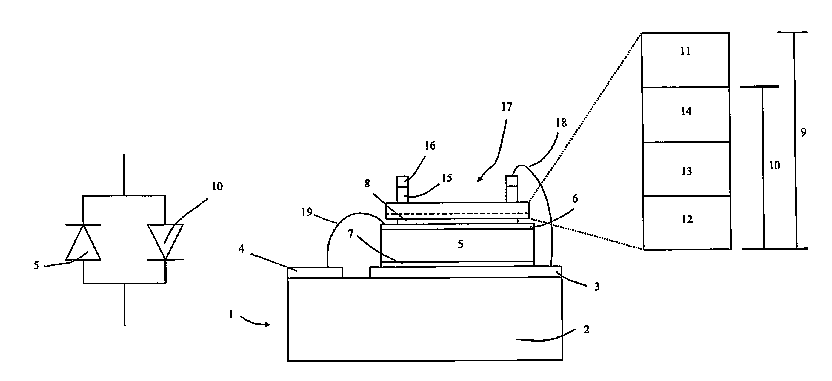
[0038]The embodiments set forth below represent the necessary information to enable those skilled in the art to practice the invention and illustrate the best mode of practicing the invention. Upon reading the following description in light of the accompanying drawing figures, those skilled in the art will understand the concepts of the invention and will recognize applications of these concepts not particularly addressed herein. It should be understood that these concepts and applications fall within the scope of the disclosure and the accompanying claims.

[0039]Shown in FIG. 1 is a semiconductor structure 1 according to the invention in cross section. This semiconductor structure 1 of this embodiment is a light emitting structure. The light emitting structure 1 comprises a package heatsink 2. Arranged on the heatsink 2 are first and second electrical connections 3,4. These connections schematically represent the packaging of the device.

[0040]The structure further comprises a silico...


PUM


Abstract

A semiconductor structure having an electrically conducting silicon substrate and a GaN semiconductor device separated from the substrate by a buffer layer is provided. The buffer layer electrically connects the silicon substrate with the GaN semiconductor device. In addition, a GaN LED arranged in a flip chip orientation on the buffer layer on the substrate is provided.

Description

FIELD OF THE INVENTION[0001]This application claims priority to UK patent application number 0902558.6, filed Feb. 16, 2009, the disclosure of which is incorporated herein by reference in its entirety.[0002]The present invention relates to a semiconductor structure and a method of manufacture thereof. More particularly, but not exclusively, the present invention relates to a semiconductor structure comprising an electrically conducting silicon substrate and a GaN semiconductor device separated from the substrate by a buffer layer. The substrate and semiconductor device are in electrical contact through the buffer layer. More particularly, but not exclusively, the present invention relates to a GaN LED arranged in a flip chip orientation on the buffer layer on the substrate. In a further aspect, the present invention relates to a method of manufacture of such a structure.BACKGROUND OF THE INVENTION[0003]GaN semiconductor devices grown on high resistivity silicon or silicon carbide su...

Claims


Application Information

Patent Timeline
IPC IPC(8): H01L33/04H01L29/15H01L33/12
CPCH01L21/02381H01L21/0243H01L21/02433H01L21/02458H01L21/0251H01L21/0254H01L2924/12032H01L33/007H01L33/0079H01L2224/48091H01L2224/73265H01L25/167H01L2924/00014H01L2224/48237H01L33/0093H01L2924/00H01L33/32H01L33/343
Inventor O'KEEFE, MATTHEW F.
Owner QORVO US INC
Why Eureka
Try Eureka