

Elemental Stacked Image Sensor
- Summary
- Abstract
- Description
- Claims
- Application Information
AI Technical Summary
Benefits of technology
Problems solved by technology
Method used
Image

Examples
Embodiment Construction
[0016]Novel Devices of the Invention.
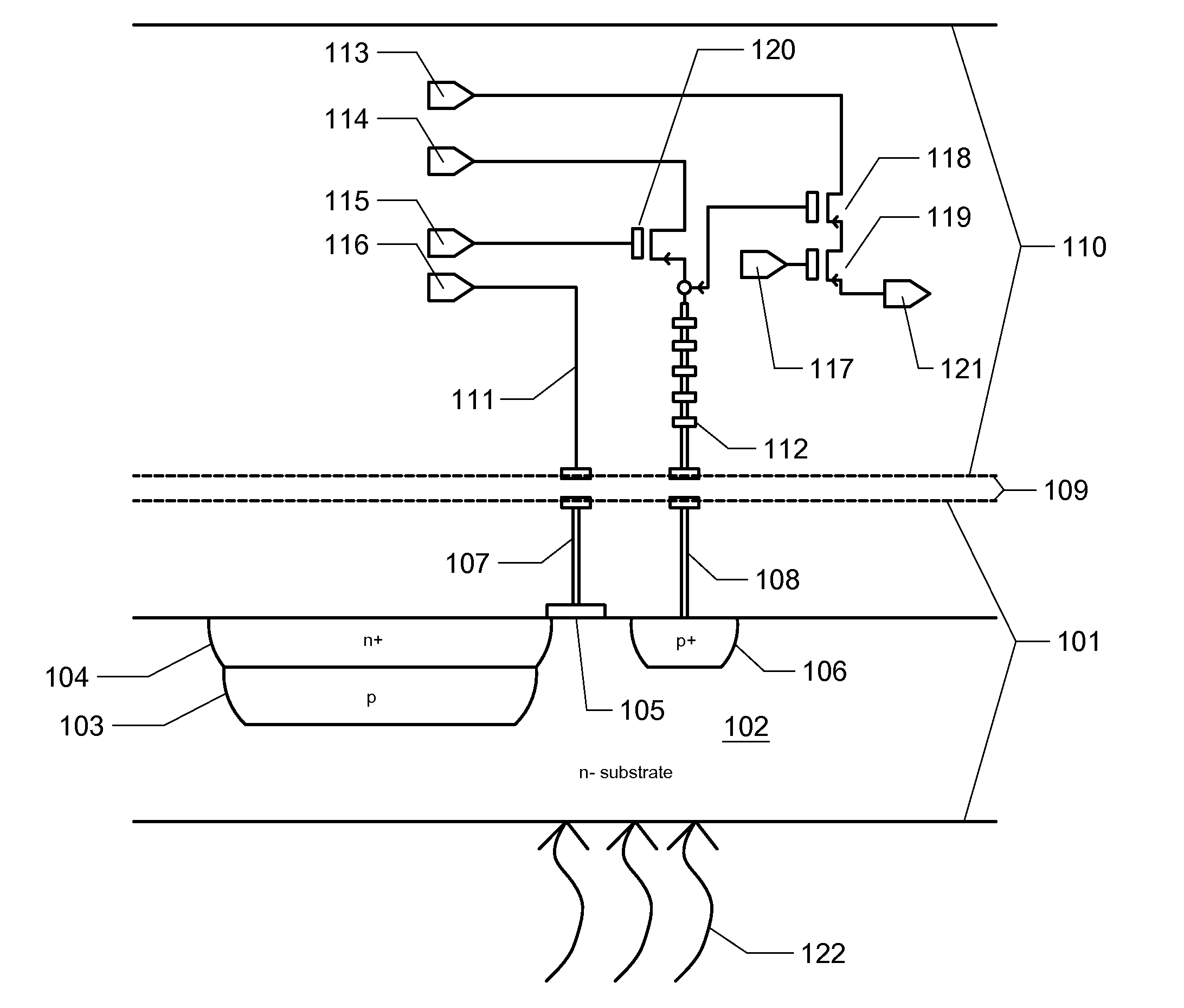
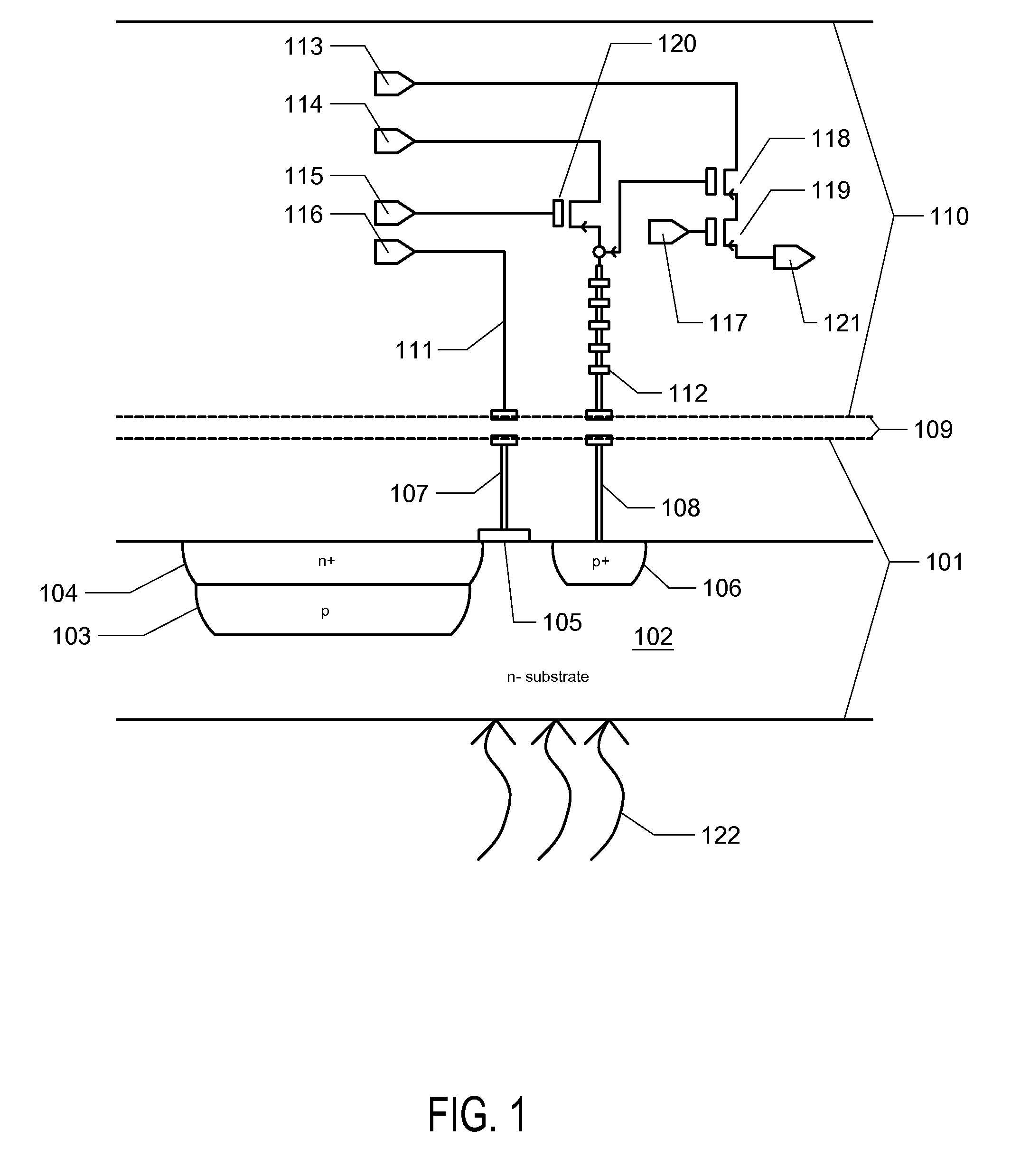
[0017]In one aspect, the invention encompasses novel pixel devices utilizing stacked, bonded wafers to create functional pixels, i.e. each pixel being a discreet photosensor element capable of converting incident light to charge, converting charge to a readout signal, and outputting such signal to a memory or signal processing component. In one embodiment, the stacked pixel of the invention comprise a photodiode, a transfer gate, and two interconnects, which are fabricated on a first wafer, while the remaining components required for pixel function are fabricated on a second wafer, as illustrated in FIG. 1. The two wafers are then aligned and bonded to create a functional photosensor element.
[0018]Reference will be made to pixel components residing on a first and a second wafer, and the description herein will be directed to the configuration of the components making up each individual pixel. It will be understood that components of multiple pixe...
PUM
 Abstract
Description
Claims
Application Information