Pixel structure, touch display panel and liquid crystal display

a liquid crystal display and pixel structure technology, applied in the field of pixel structure, touch display panel and liquid crystal display, can solve the problems of restricted viewing angle, disorderly arrangement, certain undesirable effects, etc., and achieve the effect of shortening the structure of the pixel structure of the pixel field switching and good restoration efficiency

Active Publication Date: 2010-09-16
AU OPTRONICS CORP
View PDF17 Cites 36 Cited by
  • Summary
  • Abstract
  • Description
  • Claims
  • Application Information

AI Technical Summary

Benefits of technology

[0009]Accordingly, the present invention is directed to a pixel structure for shortening the restore time of the disturbed liquid crystal molecules of a fringe field switching pixel structure.
[0010]The present invention is further directed to a touch display panel for improving the restore efficiency of the liquid crystal molecules after the touch display panel is pressed.
[0011]The present invention is again directed to a liquid crystal display having good quality.
[0017]The present invention adopts the design of connecting patterns so that at least a part of the slits of the fringe field switching pixel structure is shortened. Accordingly, the disorder arrangement of the liquid crystal molecules caused by a user's pressing can be restored rapidly when the fringe field switching pixel structure applied to a touch display panel. In another word, the present invention provides not only a pixel structure having wide viewing angle display effect and the liquid crystal display having the same, but also a pixel structure design with the liquid crystal molecules having good restore efficiency.

Problems solved by technology

However, the liquid crystal display still has a problem of restricted viewing angle.
However, certain undesirable effect may occur when the liquid crystal display having the pixel structure 100 attached with a touch panel to form a touch display panel.
For example, the liquid crystal molecules of the liquid crystal display may be disturbed and thus disorderly arrange when a user press the above-mentioned touch display panel.
Accordingly, the phenomenon of uneven brightness may occur at the place surrounding the touch point and the judgments of the touch input or the writing input of the touch panel may be harmfully influenced.

Method used


Image

  • Pixel structure, touch display panel and liquid crystal display
  • Pixel structure, touch display panel and liquid crystal display
  • Pixel structure, touch display panel and liquid crystal display

Examples


Embodiment Construction

[0030]Reference will now be made in detail to the present embodiments of the invention, examples of which are illustrated in the accompanying drawings. Wherever possible, the same reference numbers are used in the drawings and the description to refer to the same or like parts.

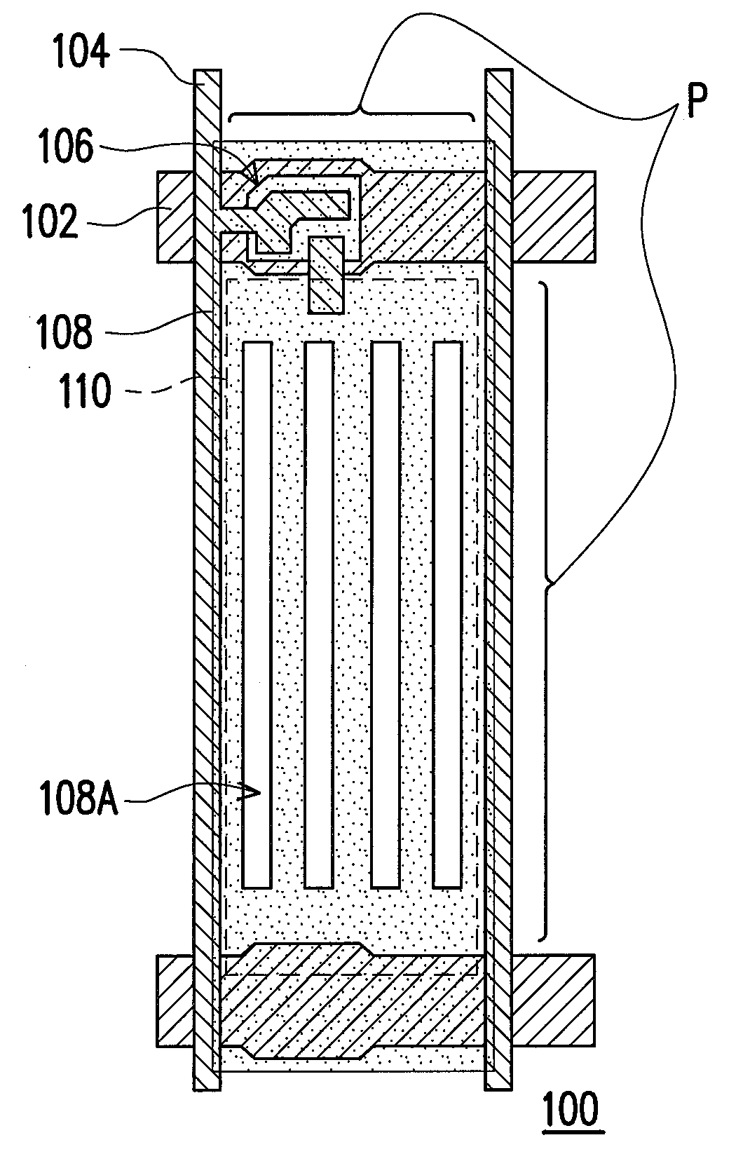
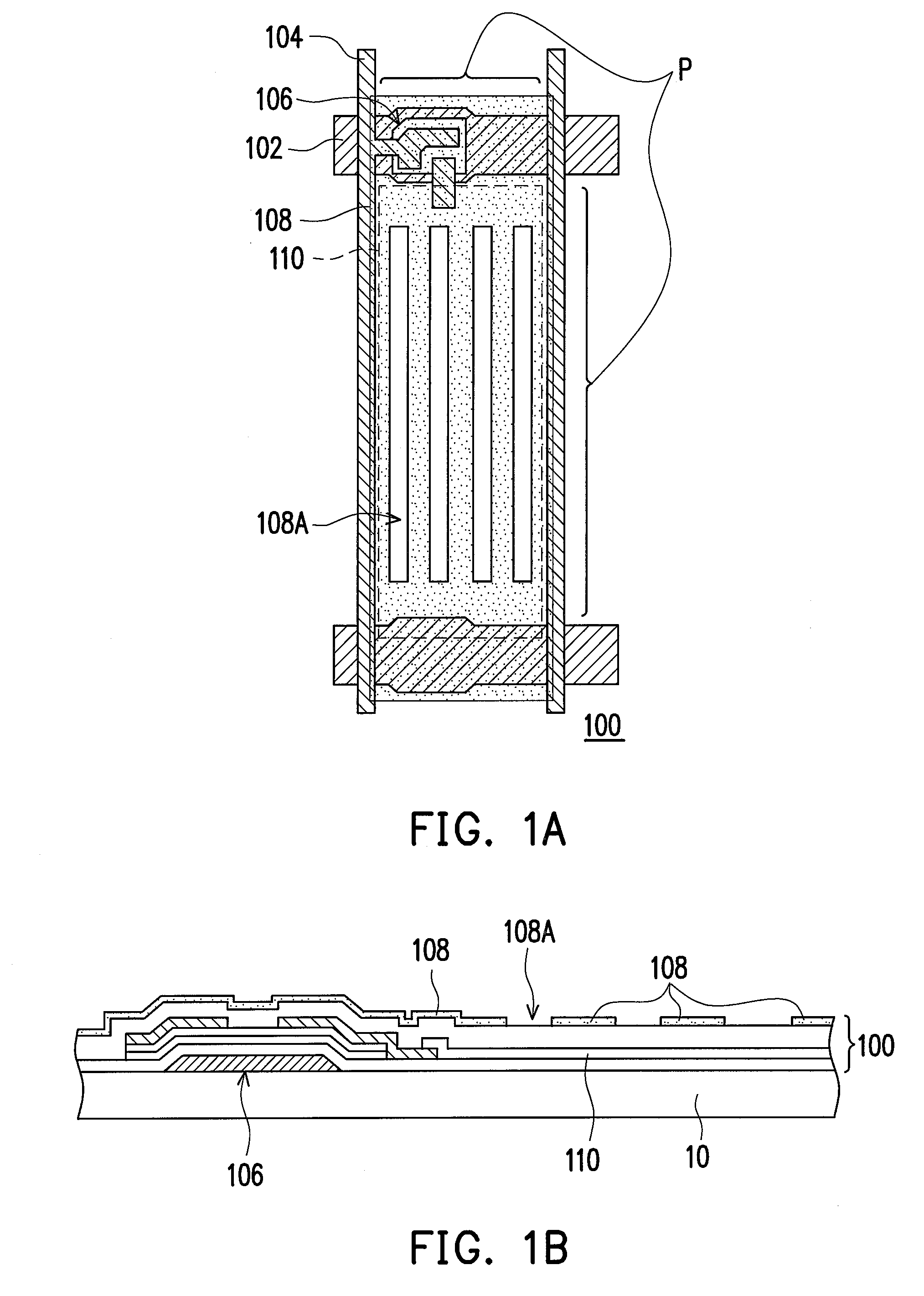
[0031]According to the above-mentioned conventional art, the pixel structure 100 as shown in FIG. 1A is capable of providing the fringe field effect to achieve the wide viewing angle display effect. However, the pixel structure 100 has narrow and long slits 108A and thus a problem that the restore time of the liquid crystal molecules is restricted by the length of the slits 108A when the pixel structure 100 is applied to a touch display panel is generated. Accordingly, for rendering the liquid crystal molecules have better restore efficiency without significantly modifying the original design of the pixel structure 100, the present invention provides the following fringe field switching pixel structures as exa...


PUM


Abstract

A pixel structure disposed on a substrate including a scan line, a data line, an active element, a first electrode, and a second electrode is provided. The scan line and the data line are intersected to define a rectangular pixel area. The active element is electrically connected to the scan line and the data line. The first electrode has stripe patterns and connecting patterns located in the rectangular pixel area. Each connecting pattern is connected to the central parts or the parts near the central parts of two adjacent stripe patterns to demarcate or define two silts between the two adjacent stripe patterns. The extending direction of the slits is intersected to the rectangle length of the rectangular pixel area by an angle θ wherein 0°≦θ<45°. The second electrode is located between the first electrode and the substrate and part of the second electrode is exposed by the slits.

Description

CROSS-REFERENCE TO RELATED APPLICATION[0001]This application claims the priority benefit of Taiwan application serial no. 98107894, filed on Mar. 11, 2009. The entirety of the above-mentioned patent application is hereby incorporated by reference herein and made a part of specification.BACKGROUND OF THE INVENTION[0002]1. Field of the Invention[0003]The present invention generally relates to a pixel structure, a touch display panel and a liquid crystal display, in particular, to a fringe field switching pixel structure, a touch display panel and a liquid crystal display.[0004]2. Description of Related Art[0005]Recently, with the optoelectronic technology and the technology of manufacturing semiconductor maturing, the development of the flat panel display is vigorous promoted. The liquid crystal display gradually replaces the conventional cathode ray tube display based on the advantages of low operation voltage, non-radiation, light weight and small volume, and thus becomes the main s...

Claims


Application Information

Patent Timeline
Patent Type & Authority Applications(United States)
IPC IPC(8): G06F3/041H05K1/00
CPCG02F1/13338G02F1/134363G06F3/0412G02F2001/134372G02F2001/134318G02F1/134318
Inventor LU, YING-CHICHAI, CHIH-YUNLI, MING-CHUNHUANG, HONG-JILEE, SEOK-LYUL
Owner AU OPTRONICS CORP
Why Eureka
Try Eureka