Nonvolatile semiconductor memory device and method of resetting the same

a non-volatile semiconductor and memory device technology, applied in the direction of digital storage, static storage, instruments, etc., can solve the problems of higher erroneous setting and higher erroneous setting problem

Active Publication Date: 2010-09-16
KIOXIA CORP
View PDF2 Cites 18 Cited by
  • Summary
  • Abstract
  • Description
  • Claims
  • Application Information

AI Technical Summary

Benefits of technology

[0012]A nonvolatile semiconductor memory device according to an aspect of the present invention includes: a semiconductor substrate; a plurality of memory cell arrays stacked on the semiconductor substrate and including a plurality of first wires, a plurality of second wires formed so as to cross the first wires, and memory cells disposed at intersections of the first wires and the second wires and each having a rectifier element and a variable resistive element connected in series; and a control circuit configured to selectively drive the first wires and the second wires, the control circuit executing a resetting operation to change a state of the variable resistive element from a low resistance state to a high resistance state, and at a time of executing the resetting operation, the control circuit increasing a pulse voltage to be applied to the variable resistive element to a first voltage, and then decreasing the pulse voltage to a second voltage lower than the first voltage and higher than the ground voltage.
[0013]Another aspect of the present invention provides a method of resetting a nonvolatile semiconductor memory device including a plurality of memory cell arrays stacked on a semiconductor substrate and including a plurality of first wires, a plurality of second wires formed so as to cross the first wires, and memory cells disposed at intersections of the first wires and the second wires and each having a rectifier element and a variable resistive element connected in series, the method comprising: at a time of executing resetting operation to change a state of the variable resistive element from a low resistance state to a high resistance state, increasing a pulse voltage to be applied to the variable resistive element to a first voltage, and then decreasing the pulse voltage to a second voltage lower than the first voltage and higher than the ground voltage.

Problems solved by technology

That is, erroneous setting occurs.
In this case, however, the possibility that the reset voltage VRESET becomes close to the set voltage VSET and it causes the erroneous setting problem becomes higher.

Method used


Image

  • Nonvolatile semiconductor memory device and method of resetting the same
  • Nonvolatile semiconductor memory device and method of resetting the same
  • Nonvolatile semiconductor memory device and method of resetting the same

Examples


first embodiment

Schematic Configuration of Nonvolatile Semiconductor Memory Device According to First Embodiment

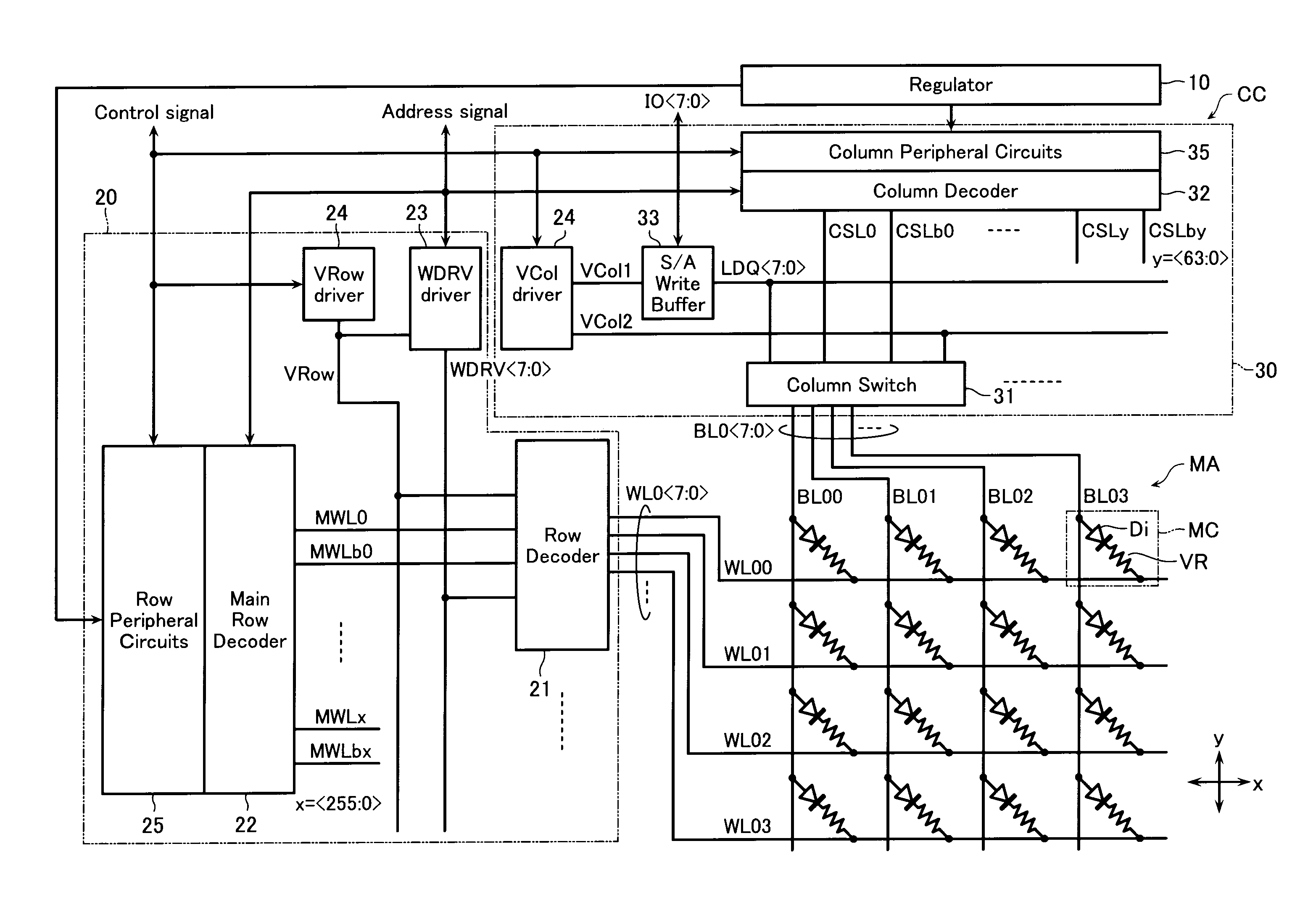
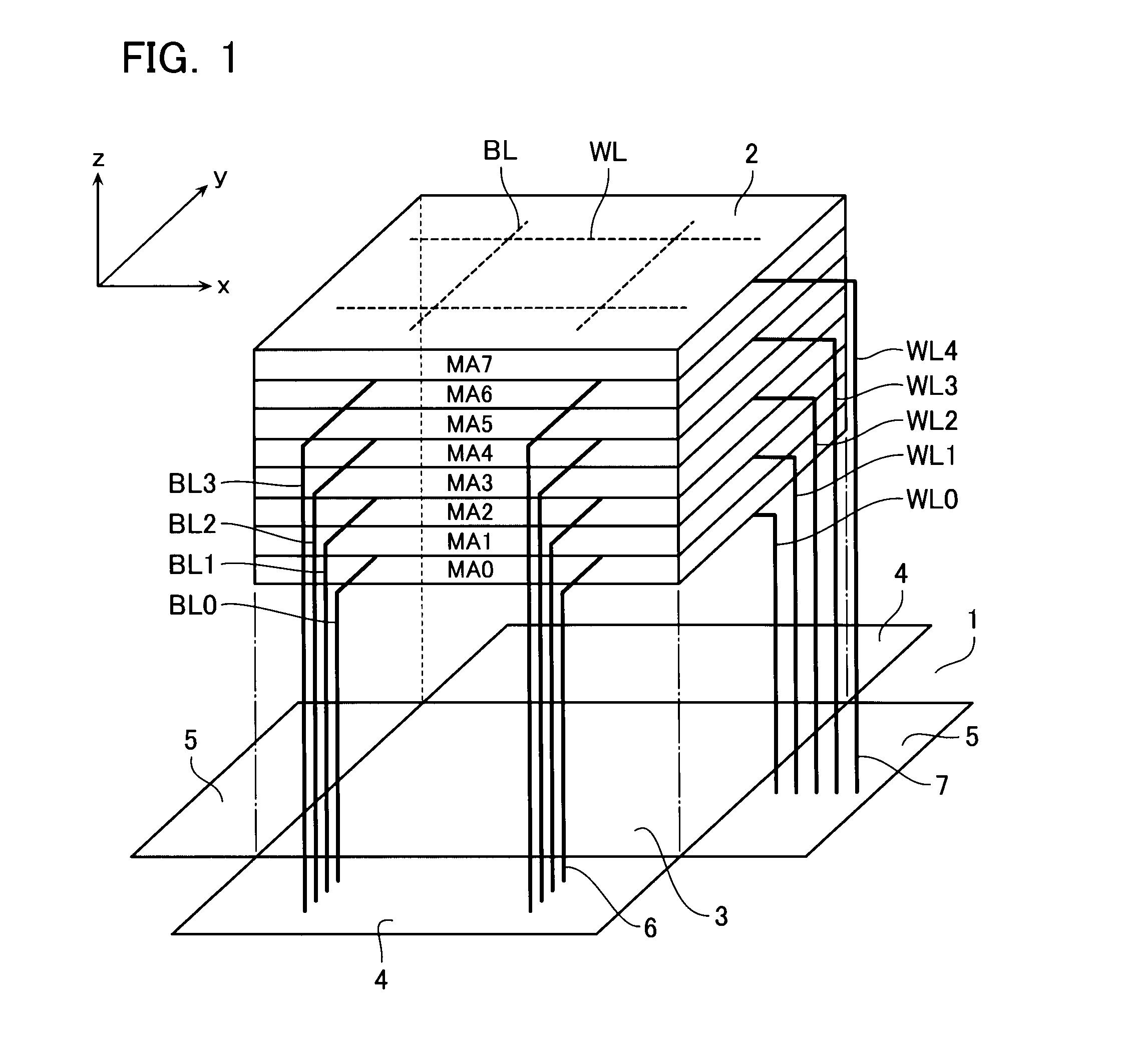
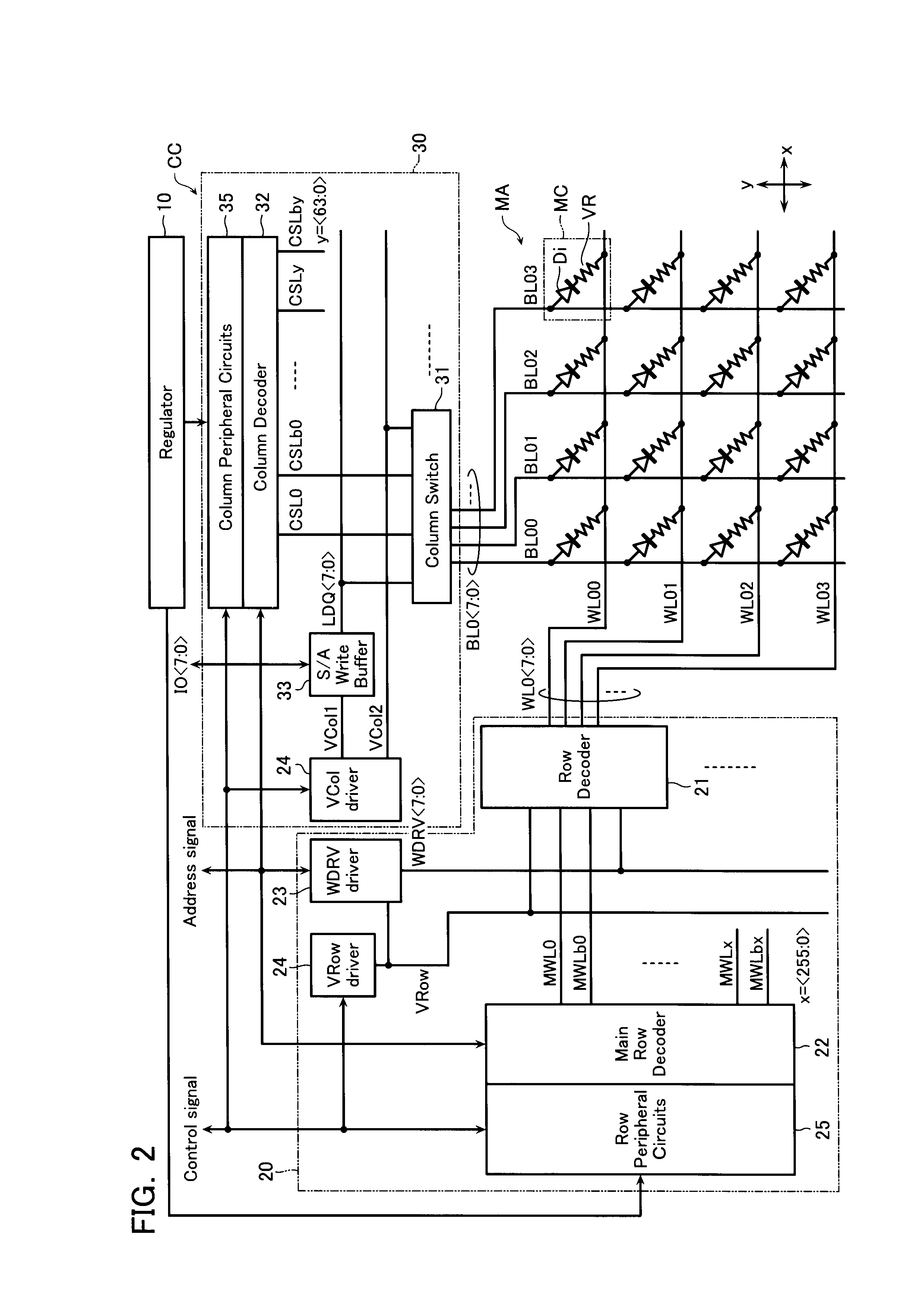
[0034]FIG. 1 shows a basic configuration of a nonvolatile semiconductor memory device according to a first embodiment of the invention, that is, a configuration of a wiring region 3 in which wires such as a global bus above a semiconductor substrate 1 are formed, and a memory block 2 stacked on the wiring region 3.

[0035]As shown in FIG. 1, in the example, the memory block 2 is made of eight memory cell arrays MA0 to MA7. As will be described later, each memory cell array MA shares a bit line or a word line with other memory cell arrays which are neighboring in a vertical direction. That is, one word line and one bit line are not connected to only a memory cell in one memory cell array but are connected to memory cells in two memory cell arrays which are neighboring in the vertical direction.

[0036]The semiconductor substrate 1 just below the memory block 2 is provided with the wiring regio...

second embodiment

Operation of Nonvolatile Semiconductor Memory Device According to Second Embodiment

[0104]Referring now to FIG. 16, the operation of the nonvolatile semiconductor memory device according to a second embodiment will be described. FIG. 16 is a timing chart showing a resetting operation of the nonvolatile semiconductor memory device according to the second embodiment. Only the resetting operation in the nonvolatile semiconductor memory device according to the second embodiment is different from that of the first embodiment. In the second embodiment, the same reference numerals are designated to components similar to those of the first embodiment and their description will not be repeated.

[0105]First, as shown in FIG. 16, at time t21, the control circuit CC changes the voltage of the selected bit line BL to a shape having “m” steps (m is an integer) and increases it to the voltage VRESET_pre. Next, at time t22, the control circuit CC changes the voltage of the selected bit line BL to a s...

third embodiment

Operation of Nonvolatile Semiconductor Memory Device According to Third Embodiment

[0110]Referring now to FIG. 17, the operation of the nonvolatile semiconductor memory device according to a third embodiment will be described. FIG. 17 is a timing chart showing a resetting operation of the nonvolatile semiconductor memory device according to the third embodiment. Only the resetting operation in the nonvolatile semiconductor memory device according to the third embodiment is different from that of each of the first and second embodiments. In the third embodiment, the same reference numerals are designated to components similar to those of the first and second embodiments and their description will not be repeated.

[0111]First, as shown in FIG. 17, at time t31, the control circuit CC increases the pulse voltage to be applied to the selected bit line BL1 to the voltage VRESET_pre. Next, at time t32, the control circuit CC changes the voltage of the selected bit line BL1 in a comb-teeth-sh...


PUM


Abstract

A nonvolatile semiconductor memory device includes: a plurality of memory cell arrays stacked on a semiconductor substrate and including a plurality of first wires, a plurality of second wires and memory cells disposed at intersections of the first wires and the second wires and having a rectifier element and a variable resistive element are connected in series; and a control circuit configured to selectively drive the first wires and the second wires. The control circuit executes a resetting operation to change a state of the variable resistive element from a low resistance state to a high resistance state. At a time of executing the resetting operation, the control circuit increases a pulse voltage to be applied to the variable resistive element to a first voltage, and then decreases the pulse voltage to a second voltage lower than the first voltage and higher than the ground voltage.

Description

CROSS-REFERENCE TO RELATED APPLICATIONS[0001]This application is based upon and claims the benefit of priority from the prior Japanese Patent Application No. 2009-59492, filed on Mar. 12, 2009, the entire contents of which are incorporated herein by reference.BACKGROUND OF THE INVENTION[0002]1. Field of the Invention[0003]The present invention relates to a nonvolatile semiconductor memory device that writes data in a nonvolatile manner by applying a voltage to a variable resistive element and a method of resetting the same.[0004]2. Description of the Related Art[0005]In recent years, as nonvolatile memory devices, a ReRAM and a PCRAM gather attention as memories succeeding a flash memory. The ReRAM and the PCRAM store information of a resistance value of an electrically-rewritable variable resistive element in a nonvolatile manner. A variable resistive element as a storage element of the ReRAM has an electrode / metal oxide (bi-metallic or ternary-metallic oxide) / electrode structure. ...

Claims


Application Information

Patent Timeline
Patent Type & Authority Applications(United States)
IPC IPC(8): G11C11/00G11C5/14
CPCG11C13/0061G11C13/0002G11C13/0038G11C13/0064G11C16/20G11C16/30
Inventor MAEJIMA, HIROSHIOKUKAWA, YUKI
Owner KIOXIA CORP
Why Eureka
Try Eureka