

Power-supply-noise cancelling circuit and solid-state imaging device
a technology of power supply and noise cancelling circuit, which is applied in the direction of color television details, television systems, instruments, etc., can solve the problems of actual signal components, read levels may not be extracted, and resolution may be degraded accordingly
- Summary
- Abstract
- Description
- Claims
- Application Information
AI Technical Summary
Benefits of technology
Problems solved by technology
Method used
Image

Examples
first embodiment
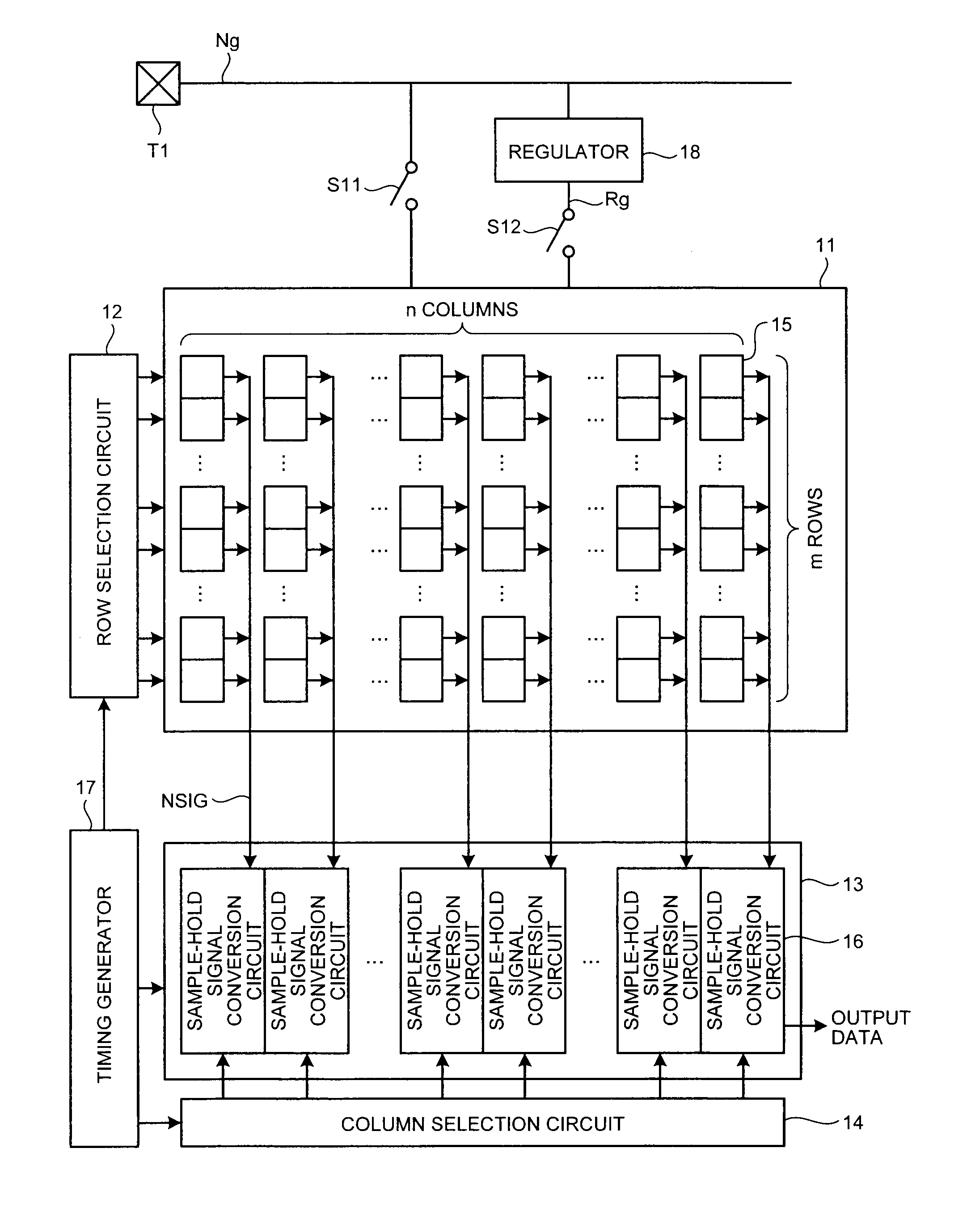
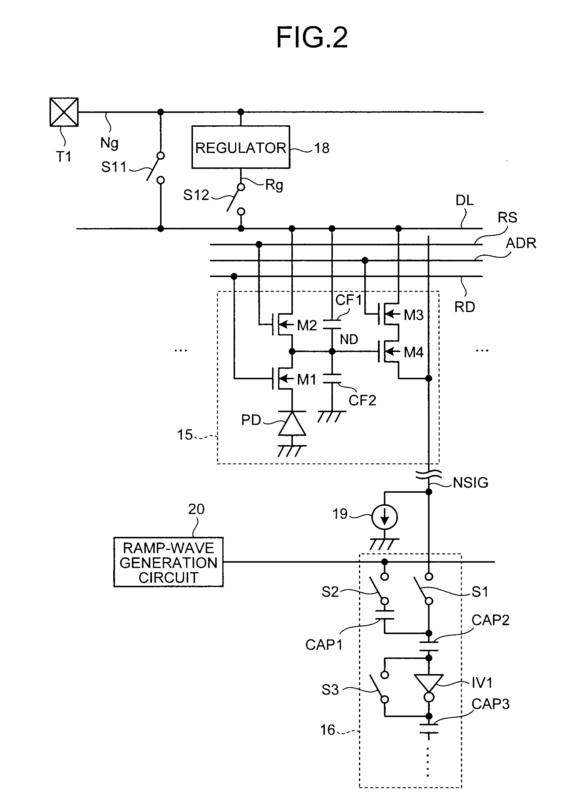
[0027]FIG. 1 is a block diagram of a general configuration of a CMOS image sensor to which a power-supply-noise cancelling circuit according to a first embodiment of the present invention is applied.
[0028]In FIG. 1, the CMOS image sensor includes a pixel array 11, a row selection circuit 12, a sample-hold signal conversion circuit group 13, a column selection circuit 14, a timing generator 17, a regulator 18, switches S11 and S12, and a power supply terminal T1. In the pixel array 11, pixels 15 that perform photoelectric conversion are arrayed in m rows and n columns (m and n are integers equal to or larger than 1). The row selection circuit 12 is able to select a row in which the pixel 15 to be a read target is arrayed. The column selection circuit 14 is able to select a column in which the pixel 15 to be the read target is arrayed. In the sample-hold signal conversion circuit group 13, sample-hold signal conversion circuits 16 are arranged for respective columns of the array of th...
second embodiment
[0061]FIG. 6 is a block diagram of a general configuration of a CMOS image sensor to which a power-supply-noise cancelling circuit according to a second embodiment of the present invention is applied.
[0062]In FIG. 6, the CMOS image sensor includes a power supply terminal T2 in addition to the configuration of the CMOS image sensor illustrated in FIG. 1. The power supply terminal T2 is able to input a power supply voltage Ng2 having a voltage value larger than that of the power supply voltage Ng and supply the power supply voltage Ng2 to the regulator 18. The power supply voltage Ng2 may be superimposed with power supply noise.
[0063]FIG. 7 is a timing diagram illustrating signal waveforms of respective units of the CMOS image sensor when the switches S11 and S12 illustrated in FIG. 6 are turned on and off.
[0064]In FIG. 7, when the power supply voltage Ng2 is supplied to the power supply terminal T2, the power supply voltage Ng2 is output to the regulator 18. When the power supply vol...
third embodiment
[0074]FIG. 8 is a block diagram of a general configuration of a CMOS image sensor to which a power-supply-noise cancelling circuit according to a third embodiment of the present invention is applied.
[0075]In FIG. 8, the CMOS image sensor includes a booster circuit 31 in addition to the configuration of the CMOS image sensor illustrated in FIG. 1. The booster circuit 31 is able to boost the power supply voltage Ng input to the power supply terminal T1 and supply it to the regulator 18.
[0076]When the power supply voltage Ng is supplied to the power supply terminal T1, the power supply voltage Ng is output to the booster circuit 31. When the power supply voltage Ng is output to the booster circuit 31, the power supply voltage Ng is boosted, so that a power supply voltage Ng3 is generated and supplied to the regulator 18. When the power supply voltage Ng3 is supplied to the regulator 18, a power supply voltage Rg3 in which power supply noise of the power supply voltage Ng3 is suppressed...
PUM
 Abstract
Description
Claims
Application Information