Printed circuit board, manufacturing method thereof and radio-frequency device

a technology of printed circuit boards and manufacturing methods, applied in the direction of printed circuit non-printed electric components association, high frequency circuit adaptation, conductive pattern formation, etc., can solve the problems of increased risk of poor reliability, increased material cost and assembly cost, and disadvantageous competition in the realization of miniaturization, etc., to achieve the effect of pcb cost and manufacturing cost, and relatively low cos

Active Publication Date: 2010-09-23
HUAWEI TECH CO LTD
View PDF14 Cites 16 Cited by
  • Summary
  • Abstract
  • Description
  • Claims
  • Application Information

AI Technical Summary

Benefits of technology

[0016]Accordingly, the present invention is directed to a laminated single board, a manufacturing method thereof, and a radio-frequency device. A fully single board sharing and laminating design is realized for various power modules and other circuit modules, which has a low cost and can meet the requirements of a high-power radio-frequency circuit.
[0023]The PCB, the manufacturing method thereof, and the radio-frequency device in the embodiments of the present invention are highly compatible, and can meet various power and frequency requirements of the radio-frequency device. As a single board solution is adopted, various signal design requirements and PCB layout and wiring requirements can be met. Meanwhile, the PCB cost and the manufacturing cost are quite low, which can meet the requirements of large power amplification.

Problems solved by technology

Such a radio-frequency module formed by a plurality of single boards is disadvantageous in competition in terms of realizing miniaturization, low cost, high reliability, and easy assembling and maintenance.
However, during the process of implementing the present invention, the inventors found that, in such a solution of the prior art, as radio-frequency signals and power supply and control signals between the single boards are realized through connectors, cable connection, or blind-mate connection, the material cost and assembling cost are increased, and the risk of poor reliability is increased.
However, during the process of implementing the present invention, the inventors found that, in such a solution of the prior art, as the signal loss of the low-cost board material is far higher than that of the radio-frequency board material, such a solution is not applicable to high-frequency high-power situations.
In addition, as the HDI technology is adopted, the PCB manufacturing cost is higher than that in the plated through hole (PTH) technology.
Moreover, the HDI technology cannot be implemented by pressing radio-frequency board materials.
As only holes with a limited depth (for example, less than 5 mil) can be formed by laser drilling, and most radio-frequency board materials are not suitable for performing laser drilling.
However, during the process of implementing the present invention, the inventors found that, in such a solution of the prior art, as the PA adopts an embedded module, a particular connector is required to connect the power amplification module with the large PCB, so that the complexity and cost of the manufacturing and assembling processes are increased.
If the module is soldered on the large PCB by reflow soldering, the risks of poor soldering and poor reliability of solder connection may be caused due to the coplanar fitting problems.
As the large PCB adopts the HDI technology, the manufacturing cost of the PCB is rather high.
In addition, the embedded module is not suitable for the realization of a large-size PA.
In addition, as the external shape of the PA module needs to cater to the design requirements of the large PCB, the compatibility of the PA module is deteriorated, resulting in complex material relations, thereby increasing the peripheral costs of assembling, material maintenance, and the like.
All of the above solutions in the prior art have defects.
In addition, due to various reasons, in some radio-frequency devices, the demand for a high-power PA (for example, higher than 80 W) is increasingly large.
However, the above solutions fail to integrate all the high-power PA, the LNA, the power supply module, the TRX, and other circuits on the same single board, that is because the process of designing the high-power PA and the other modules on the same single board needs to meet requirements in many aspects, including loss, pin count, heat dissipation, single board thickness, partial sintering, warping control, interconnection among single boards and modules, assembling, and the like.

Method used


Image

  • Printed circuit board, manufacturing method thereof and radio-frequency device
  • Printed circuit board, manufacturing method thereof and radio-frequency device
  • Printed circuit board, manufacturing method thereof and radio-frequency device

Examples


Embodiment Construction

[0030]A detailed description of embodiments of the present invention is given below with reference to the accompanying drawings.

[0031]The present invention is described in detail below through some exemplary embodiments with reference to the accompanying drawings.

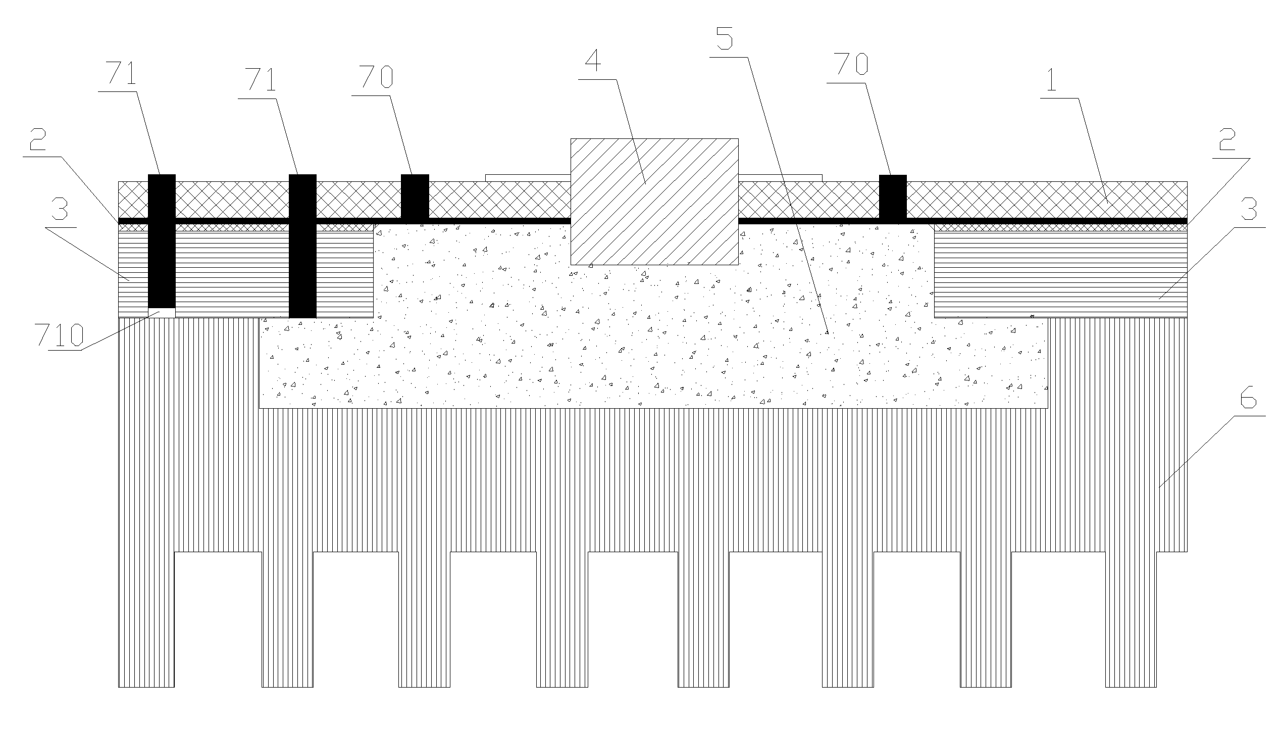
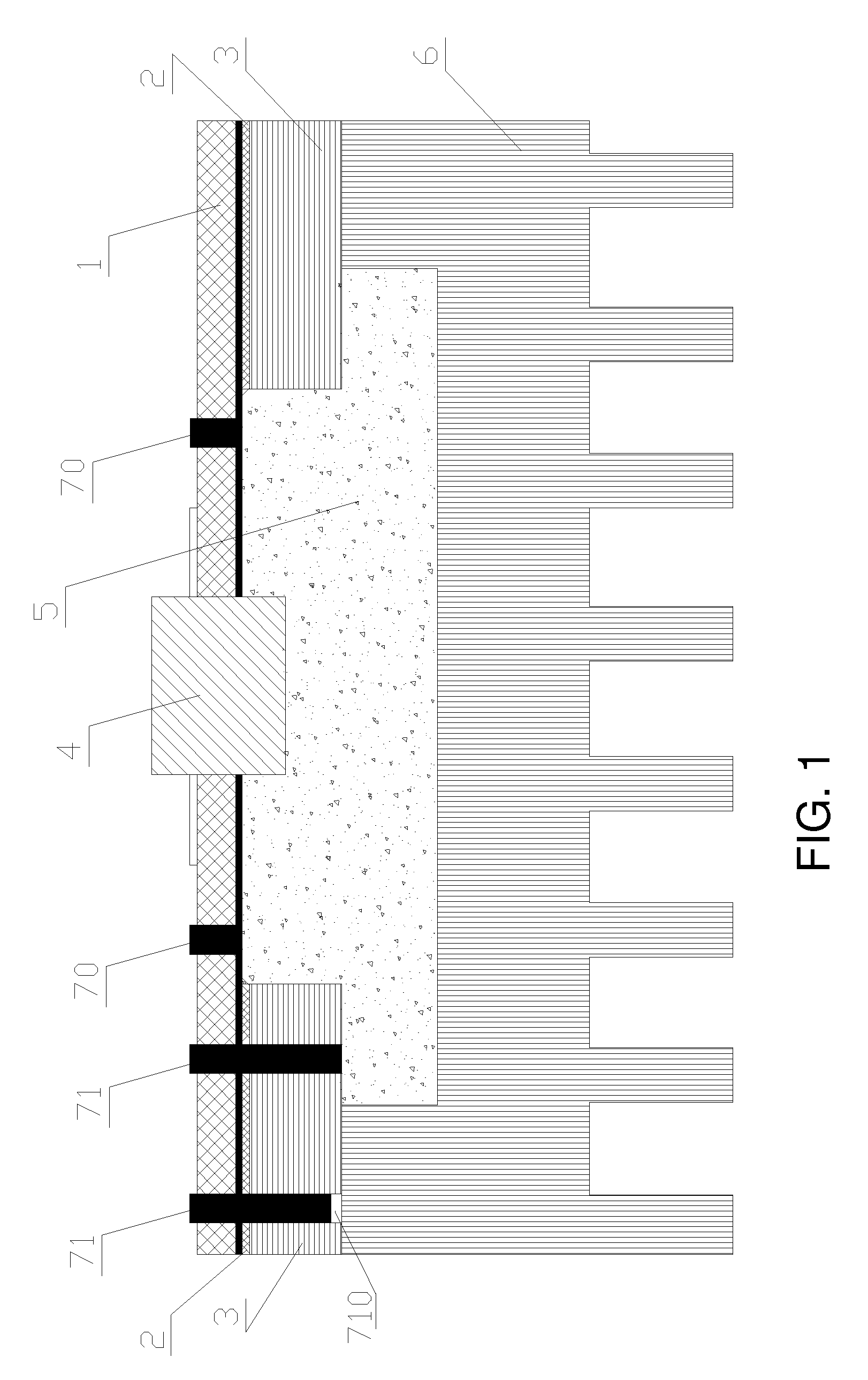
[0032]FIG. 1 is a schematic longitudinal sectional view of a PCB according to an embodiment of the present invention. In this embodiment, for ease of illustration, positions of a partially-sintered heat-dissipation metal block 5 and a heat sink 6 are both shown in the figure. The PCB includes a first board material 1, a second board material 2, and a third board material 3 sequentially pressed together. In a specific implementation, the first board material 1 is a high-frequency PCB material (for example, a radio-frequency board material), the second board material 2 is a prepreg, and the third board material 3 is a low-frequency PCB material. Each board material may be configured in more than one layer. For example, in FIG...


PUM

PropertyMeasurementUnit
depthaaaaaaaaaa
sizesaaaaaaaaaa
frequencyaaaaaaaaaa

Abstract

A printed circuit board (PCB) is provided. The PCB includes a first microwave board material, a second prepreg, and a third ordinary board material that are pressed together. The first microwave board material, the second prepreg, and the third ordinary board material are provided with an opening respectively. At least two openings have different sizes. In a region between boundaries of the at least two openings having different sizes, a borehole is provided to pass through the board material in the region. A back-drilled hole is selectively used. A radio-frequency device and a method for manufacturing a PCB are further provided. Thus, it is suitable for designing different power modules and other circuit modules on the same single board, and is compatible with the existing basic PCB manufacturing technologies, which further has a low cost, and can meet the requirements of large-power radio-frequency circuits with different frequencies.

Description

CROSS-REFERENCE TO RELATED APPLICATIONS[0001]This application is a continuation of International Application No. PCT / CN2008 / 073417, filed on Dec. 10, 2008, which claims priority to Chinese Patent Application No. 200710032455.1 filed on Dec. 14, 2007, both of which are hereby incorporated by reference in their entireties.FIELD OF THE TECHNOLOGY[0002]The present invention relates to the field of a printed circuit board (PCB), and more particularly to a PCB, a manufacturing method thereof, and a radio-frequency device.BACKGROUND OF THE INVENTION[0003]A radio-frequency module of an existing radio-frequency device, for example, a base station (BS), is generally formed by a plurality of single boards, such as transceiver (TRX) single board, low noise amplifier (LNA) single board, power amplifier (PA) single board, power supply single board, and cavity duplexer. Such a radio-frequency module formed by a plurality of single boards is disadvantageous in competition in terms of realizing mini...

Claims


Application Information

Patent Timeline
Patent Type & Authority Applications(United States)
IPC IPC(8): H05K7/00H05K3/10
CPCH05K2201/10416H05K1/0243H05K2201/09845H05K1/036H05K2203/063H05K3/0061Y10T29/49155H05K3/4688H05K1/025H05K1/182H05K2201/09745H05K1/021H05K1/024H05K1/03H05K1/11
Inventor YANG, RUIQUANSHENG, HAIQIANGLI, HONGCAI
Owner HUAWEI TECH CO LTD
Why Eureka
Try Eureka