Spin-bus for information transfer in quantum computing

a quantum computing and information transfer technology, applied in computing, semiconductor devices, instruments, etc., can solve the problems of long-range coupling, putting error correction out of reach, and affecting the algorithm with sub-exponential speedup, and achieve excellent decoherence properties and maximize bus speed

Active Publication Date: 2010-09-23
WISCONSIN ALUMNI RES FOUND
View PDF6 Cites 29 Cited by
  • Summary
  • Abstract
  • Description
  • Claims
  • Application Information

AI Technical Summary

Benefits of technology

[0009]The spin bus is formed of a large clustered qubit or spin chain, with interactions between the individual spins being strong and always on. The ground-state manifold of the spin cluster is doubly degenerate and desirably has an excitation gap that is as large as possible. One spin bus design which meets these criteria is composed of is an electron spin bus having an odd number of spins, wherein the couplings between the spins in the chain are equal or substantially equal. In the case where the “spin” cluster actually comprises an electron spin cluster, has a total spin-1 / 2, as in a conventional spin qubit. Other designs are possible, however. For example the spin bus may the spin bus may have an even number of spins with specially chosen couplings between the qubits in the chain. Relevant considerations, as they apply to a spin bus having a ring configuration are discussed in Meier et al., Phys. Rev. B, vol. 68, pp. 134417-1-15 (2003), the entire disclosure of which is incorporated herein by reference.
[0010]The effective spin of the bus interacts with other spins or cluster qubits via exchange coupling. Because information is transmitted on the bus through the spin channel, the information is largely decoupled from its charge environment, providing excellent decoherence properties. In the spin bus quantum computing (QC) architecture in accordance with the invention, only one or at most a few very large clusters are used to form a bus, while the working qubits are comprised of individual qubits or much smaller clusters. A qubit can couple to any individual spin in the bus, as compared to cluster schemes wherein only spins at the ends of the clusters are used to couple the other clusters. In the spin bus of the invention, the spins in the bus are strongly coupled to maximize the bus speed, and the coupling is always on. The bus is not intended to store information other than for the short time required to transmit the information from source to destination. Sectors on the spin bus may be defined in which qubits storing information are coupled to the bus such that information can be transmitted to or received from the bus to communicate with a readout sector at a remote location on the bus which allows a readout of the information to conventional electronic circuits.
[0011]In one embodiment the spin bus QC architecture of the invention includes a spin bus formed of multiple strongly coupled and always on quantum dots that define a string of spin quantum dots. A plurality of information bearing qubits are formed as quantum dots with each qubit adjacent a quantum dot of the spin bus. Electrodes are formed adjacent to the information bearing qubits and the spin bus quantum dots to allow control of the establishment and breaking of coupling between each information bearing qubit and the spin bus quantum dot adjacent to it.
[0012]The QC architecture may be formed in a multi-layer semiconductor structure which includes a bottom semiconductor layer, a top semiconductor layer, and an intermediate quantum well layer in which the quantum dots are defined. The top and bottom layers may be formed of, e.g., SiGe, and the intermediate quantum well layer may be formed of Si, it being understood that the invention may be implemented in any other suitable semiconductor material system. The invention is not limited to such multi-layer quantum well structures. For example only, the invention may be implemented in a silicon-germanium multi-layer structure in which electrons are trapped on phosphorus ions implanted into a silicon-geranium matrix, with control of the coupling of the qubits to the spin bus implemented with the top gate electrodes. The invention is also not limited to implementation in semiconductor systems. For example, the qubits may be defined in a electrons floating above a substrate of superfluid helium wherein the electrons are trapped laterally by metal electrodes for the bus and the qubits, with coupling between the qubits and the spin bus controlled by the electrodes.

Problems solved by technology

Potential issues with such proposed systems include individual impurity spins, as well as gate operation and readout methods for the quantum dots.
While such procedures would not affect the exponential nature of algorithmic speedup for prime factorization, they could be detrimental for algorithms with sub-exponential speedup.
In particular, because of the nested structure of fault-tolerant algorithms, the absence of long-range couplings could be catastrophic, effectively putting error correction out of reach.
However, because of the physical extent of the bus, these modes have a tendency to couple more strongly to the environment than localized qubits, with a consequent effect on bus decoherence.
Additionally, it often is the case that bus modes couple rather weakly to the qubits, causing a decrease in the bus speed.
However, viable bus architectures for such quantum dot solid-state systems have been difficult to achieve because of the lack of viable bus schemes that are technologically compatible with semiconductor heterostructures.
Unfortunately, the physical realization of this scheme has apparently not been achieved, in part because this approach requires precisely positioned lasers that are extremely difficult to realize experimentally.
However, detuning also considerably reduces the speed of information transfer.
Consequently, long-range coupling remains among the chief architectural challenges for scalable spin-based quantum computing.

Method used


Image

  • Spin-bus for information transfer in quantum computing
  • Spin-bus for information transfer in quantum computing
  • Spin-bus for information transfer in quantum computing

Examples


Embodiment Construction

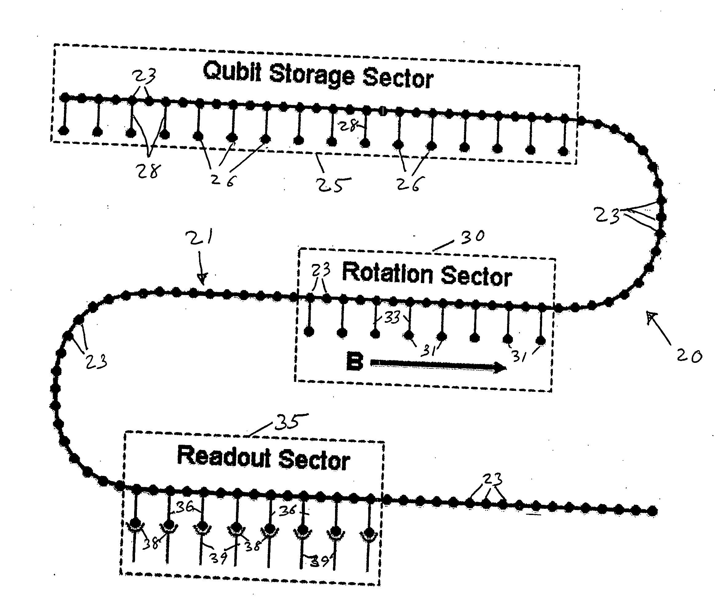
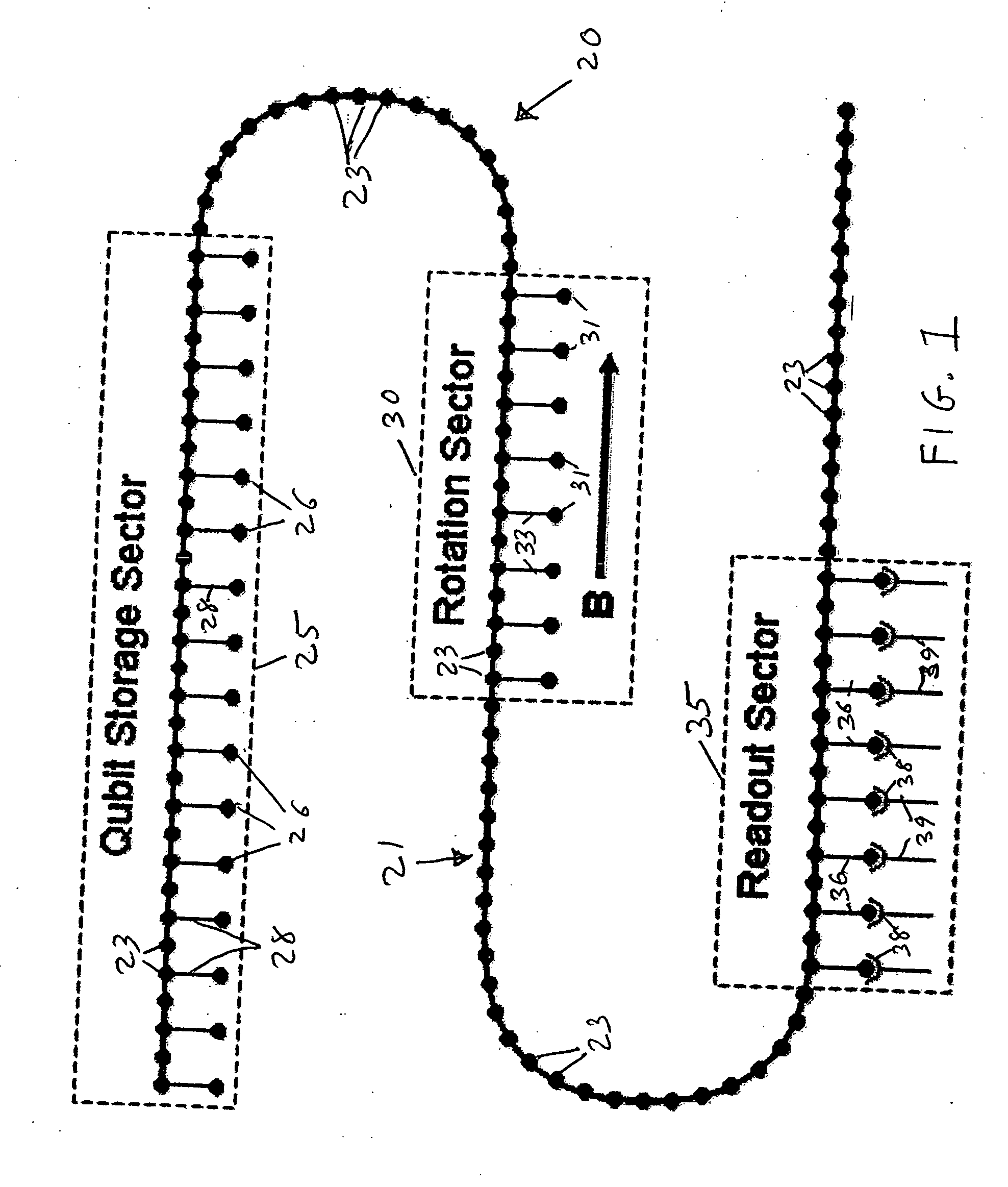
[0024]A simplified view of a spin-bus QC architecture in accordance with the invention is shown generally at 20 in FIG. 1. The QC architecture 20 may be implemented in semiconductors as well as other structures as discussed further below. The QC architecture 20 includes a main spin bus 21 formed of a string of qubits (i.e., the “bus qubits”, e.g., quantum dots) 23 which are always on and which are strongly coupled together. Information bearing working qubits can be selectively coupled to the qubits of the bus to receive information from or provide information thereto. For purposes of illustration, the spin bus QC architecture 20 includes a qubit storage sector 25 having a series of qubits 26 which are coupled to the bus 21 by couplings 28 which can be turned on and off electronically. A rotation sector 30 has qubits 31 which are selectively coupled to the spin bus 21 by couplings 33 which can be turned on and off electronically and which can be affected by a magnetic field applied f...


PUM


Abstract

A spin bus quantum computing architecture includes a spin bus formed of multiple strongly coupled and always on qubits that define a string of spin qubits. A plurality of information bearing qubits are disposed adjacent a qubit of the spin bus. Electrodes are formed to the information bearing qubits and the spin bus qubits to allow control of the establishment and breaking of coupling between qubits to allow control of the establishment and breaking of coupling between each information bearing qubit and the spin bus qubit adjacent to it. The spin bus architecture allows rapid and reliable long-range coupling of qubits.

Description

STATEMENT OF GOVERNMENT RIGHTS[0001]This invention was made with United States government support awarded by the following agencies: ARMY DAAD 19-01-1-0515 and National Science Foundation (NSF) 0130400. The United States government has certain rights in this invention.FIELD OF THE INVENTION[0002]This invention pertains generally to the field of quantum computing, quantum information processing and quantum communication.BACKGROUND OF THE INVENTION[0003]Quantum computing utilizes quantum particles to carry out computational processes. The fundamental unit of quantum information is called a quantum bit or qubit. A qubit can be both a zero and a one at the same time. An example is the spin of an electron, wherein the up or down spin can correspond to a zero, a one, or a superposition of states in which it is both up and down at the same time. Performing a calculation using the electron essentially performs the operation simultaneously for both a zero and a one. Experimental advances in ...

Claims


Application Information

Patent Timeline
Patent Type & Authority Applications(United States)
IPC IPC(8): G06F13/14
CPCG06N99/002B82Y10/00G06N10/00
Inventor FRIESEN, MARK G.
Owner WISCONSIN ALUMNI RES FOUND
Why Eureka
Try Eureka