Semiconductor device

a technology of semiconductor devices and semiconductors, applied in the direction of semiconductor devices, electrical equipment, transistors, etc., can solve the problem of increasing the power consumption of semiconductor devices

Active Publication Date: 2010-09-30
SEMICON ENERGY LAB CO LTD
View PDF105 Cites 168 Cited by
  • Summary
  • Abstract
  • Description
  • Claims
  • Application Information

AI Technical Summary

Benefits of technology

[0020]A thin film transistor is a switching element that is turned on when a certain amount of voltage (referred to as a threshold voltage (Vth)) is applied to a gate electrode and is turned off when a voltage less than the certain amount is applied. This threshold voltage (Vth) corresponds to the amount of voltage at

Problems solved by technology

If the amount of shift from 0 V is large, driving voltage is increased, wh

Method used


Image

  • Semiconductor device
  • Semiconductor device
  • Semiconductor device

Examples


embodiment 1

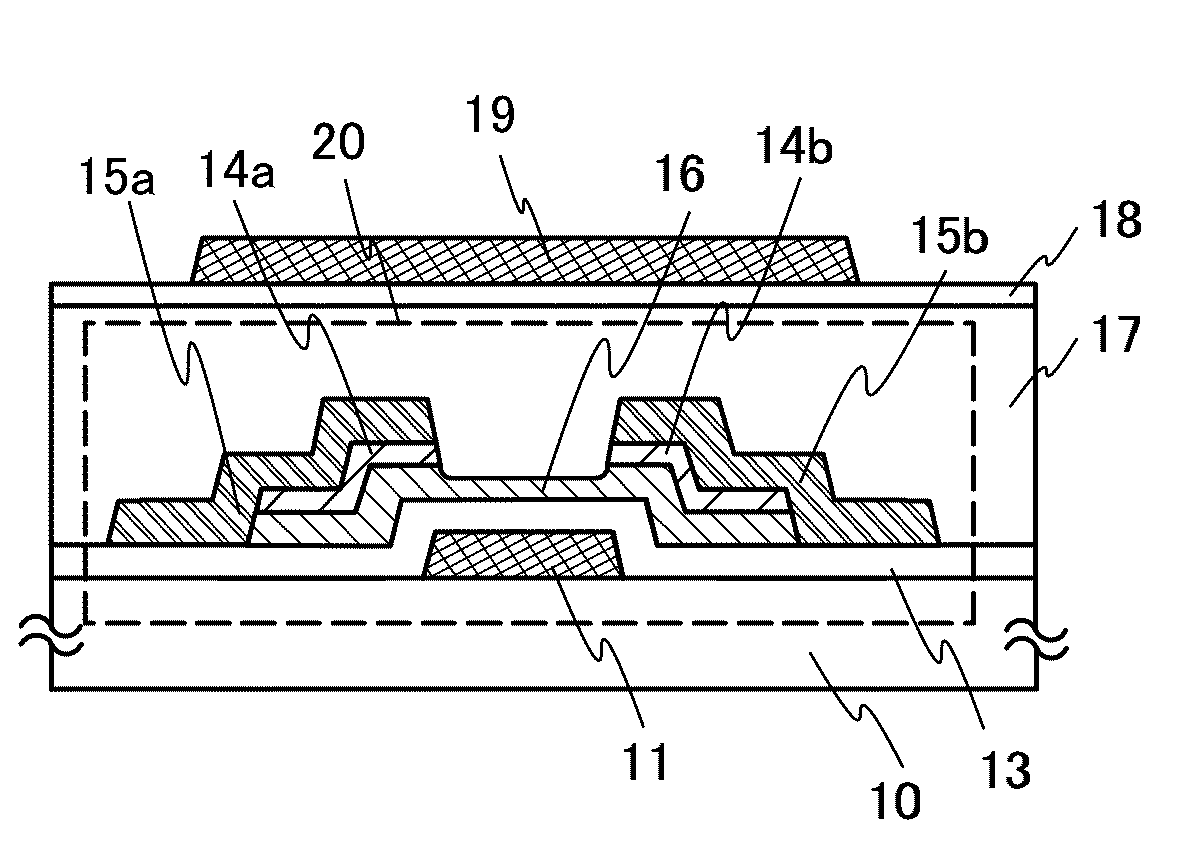
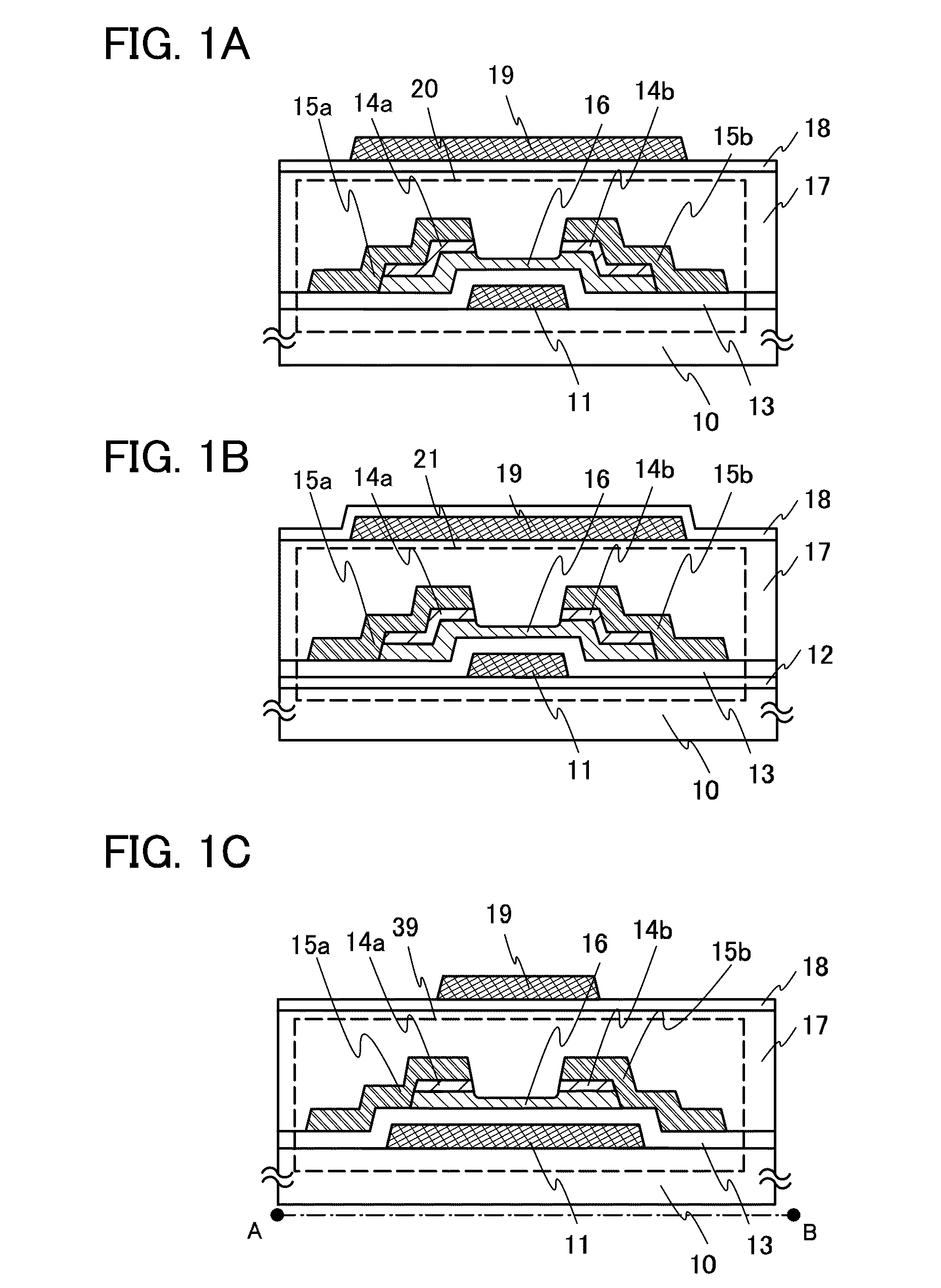
[0090]FIG. 1A is an example of a cross-sectional view of a thin film transistor in which an oxide semiconductor layer is sandwiched between two gate electrodes provided over and below the oxide semiconductor layer. This embodiment describes an example of a manufacturing method by which a thin film transistor used for a pixel portion and a driver circuit is provided over a substrate having an insulating surface.

[0091]First, a first gate electrode 11 is formed over a substrate 10 having an insulating surface. As the substrate 10 having an insulating surface, any glass substrate used in the electronics industry (also called an alkali-free glass substrate) such as an aluminosilicate glass substrate, an aluminoborosilicate glass substrate, or a barium borosilicate glass substrate, a plastic substrate with heat resistance which can withstand a process temperature in this manufacturing process, or the like can be used. In the case where the substrate 10 is mother glass, the substrate may h...

embodiment 2

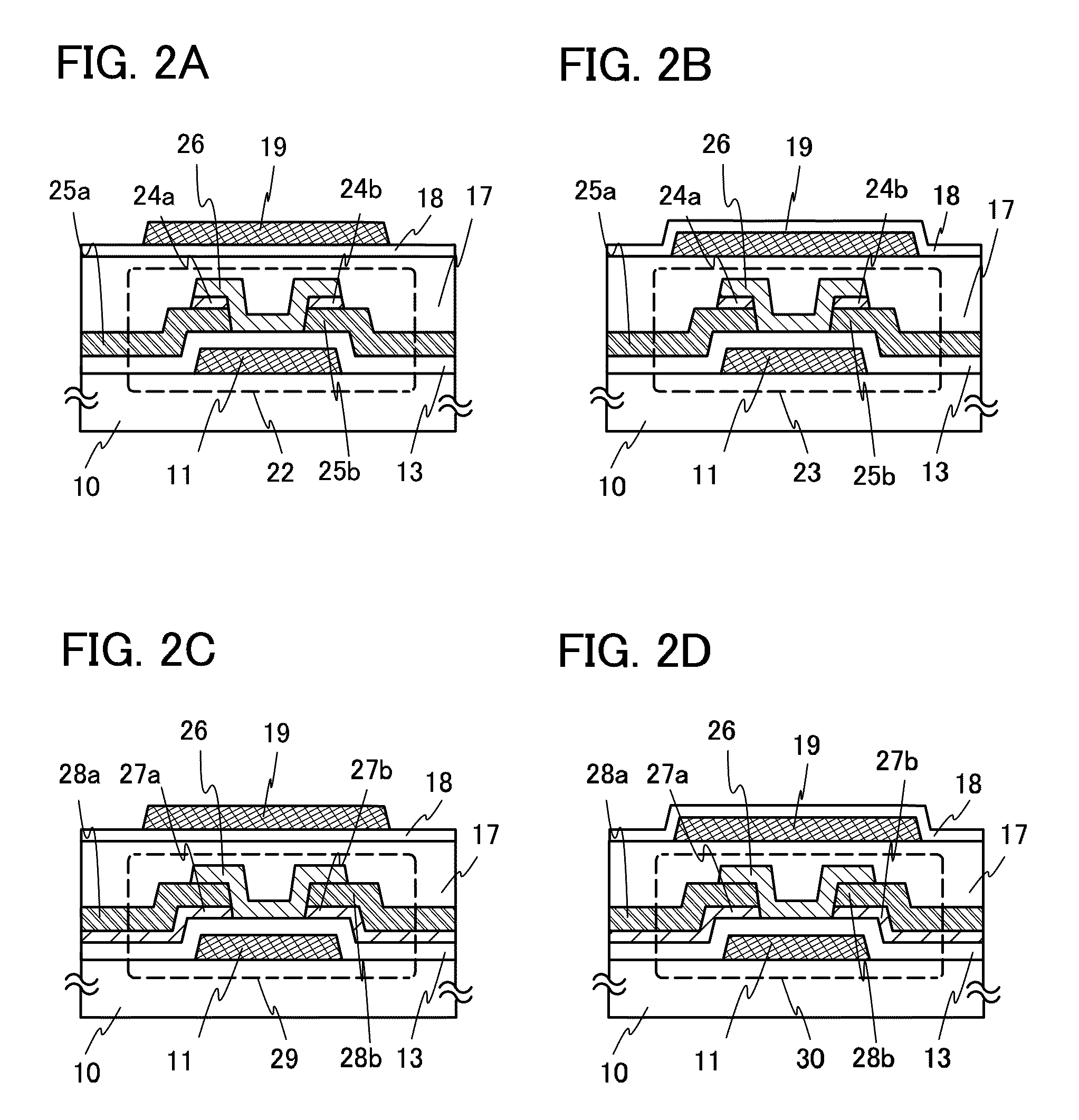
[0126]FIG. 2A is an example of a cross-sectional view of a thin film transistor in which an oxide semiconductor layer is sandwiched between two gate electrodes provided over and below the oxide semiconductor layer. This embodiment describes an example of a manufacturing method by which a thin film transistor used for a pixel portion and a driver circuit is provided over a substrate having an insulating surface.

[0127]The same steps as Embodiment 1 are employed from formation of the first gate electrode 11 over the substrate 10 having an insulating surface up to formation of the first gate insulating layer 13 covering the first gate electrode 11. Therefore, detailed description is omitted here and the same portions as those of FIG. 1A are denoted by the same reference numerals.

[0128]A conductive film is formed from a metal material over the first gate insulating layer 13 by a sputtering method or a vacuum evaporation method. In this embodiment, a three-layer structure of a Ti film, an...

embodiment 3

[0156]FIG. 3A is an example of a cross-sectional view of a thin film transistor in which an oxide semiconductor layer is sandwiched between two gate electrodes provided over and below the oxide semiconductor layer. This embodiment describes an example of a manufacturing method by which a thin film transistor used for a pixel portion and a driver circuit is provided over a substrate having an insulating surface.

[0157]Note that steps in which the first gate electrode 11 is formed over the substrate 10 having an insulating surface, the first gate insulating layer 13 covering the first gate electrode 11 is formed, and an oxide semiconductor film is formed are the same as those of Embodiment 1. Therefore, detailed description is omitted here and the same portions as those of FIG. 1A are denoted by the same reference numerals.

[0158]In this embodiment, an oxide semiconductor film over the first gate insulating layer 13 is formed using a Zn—O-based oxide semiconductor target including SiO2 ...


PUM


Abstract

The threshold voltage is shifted in a negative or positive direction in some cases by an unspecified factor in a manufacturing process of the thin film transistor. If the amount of shift from 0 V is large, driving voltage is increased, which results in an increase in power consumption of a semiconductor device. Thus, a resin layer having good flatness is formed as a first protective insulating film covering the oxide semiconductor layer, and then a second protective insulating film is formed by a sputtering method or a plasma CVD method under a low power condition over the resin layer. Further, in order to adjust the threshold voltage to a desired value, gate electrodes are provided over and below an oxide semiconductor layer.

Description

BACKGROUND OF THE INVENTION[0001]1. Field of the Invention[0002]The present invention relates to a semiconductor device having a circuit formed using a thin film transistor (hereinafter referred to as a TFT) and a manufacturing method thereof. For example, the present invention relates to an electronic appliance in which an electro-optical device typified by a liquid crystal display panel or a light-emitting display device including an organic light-emitting element is mounted as its component.[0003]Note that the semiconductor device in this specification refers to all the devices which can operate by using semiconductor characteristics. An electro-optical device, a semiconductor circuit, and an electronic appliance are all semiconductor devices.[0004]2. Description of the Related Art[0005]Various metal oxides are used for a variety of applications. Indium oxide is a well-known material and is used as a transparent electrode material which is necessary for liquid crystal displays an...

Claims


Application Information

Patent Timeline
IPC IPC(8): H01L29/786
CPCH01L27/1225H01L29/78606H01L29/7869H01L29/78648H01L29/78645H01L29/42384H10K59/1213H01L29/78618H10K59/123H01L29/42376
Inventor YAMAZAKI, SHUNPEIABE, TAKAYUKISHISHIDO, HIDEAKI
Owner SEMICON ENERGY LAB CO LTD
Why Eureka
Try Eureka