
Circuit board and manufacturing method thereof

a technology of circuit boards and manufacturing methods, applied in the field of circuit boards, can solve problems such as difficulty in controlling the depth of laser machining

Active Publication Date: 2010-10-07
UNIMICRON TECH CORP
View PDF28 Cites 24 Cited by
  • Summary
  • Abstract
  • Description
  • Claims
  • Application Information

AI Technical Summary

Benefits of technology

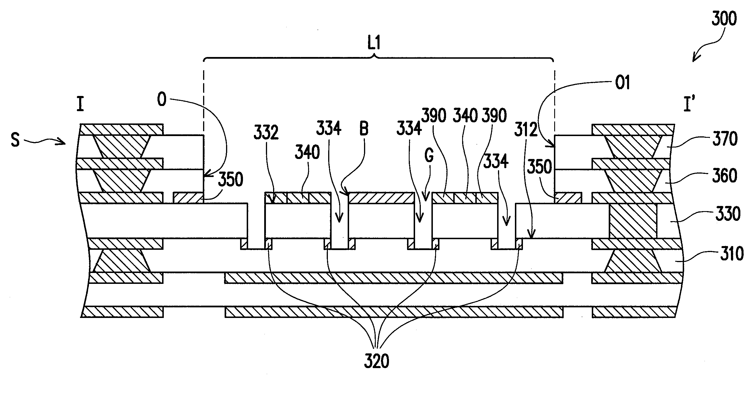
The present invention provides a circuit board with effective laser machining depth control. The circuit board includes a first dielectric layer, a first laser resistant structure, a second dielectric layer, a circuit layer, a second laser resistant structure, and a third dielectric layer. The second laser resistant structure is disposed on the first surface of the substrate and located at the periphery of the pre-removing area. The third dielectric layer is disposed on the second dielectric layer and covers the circuit layer and the second laser resistant structure. The present invention also provides a manufacturing method of the circuit board. The technical effect of the present invention is to control the depth of laser machining in the circuit board, which is achieved by effective control of the laser resistant structures and the gap between them.

Problems solved by technology

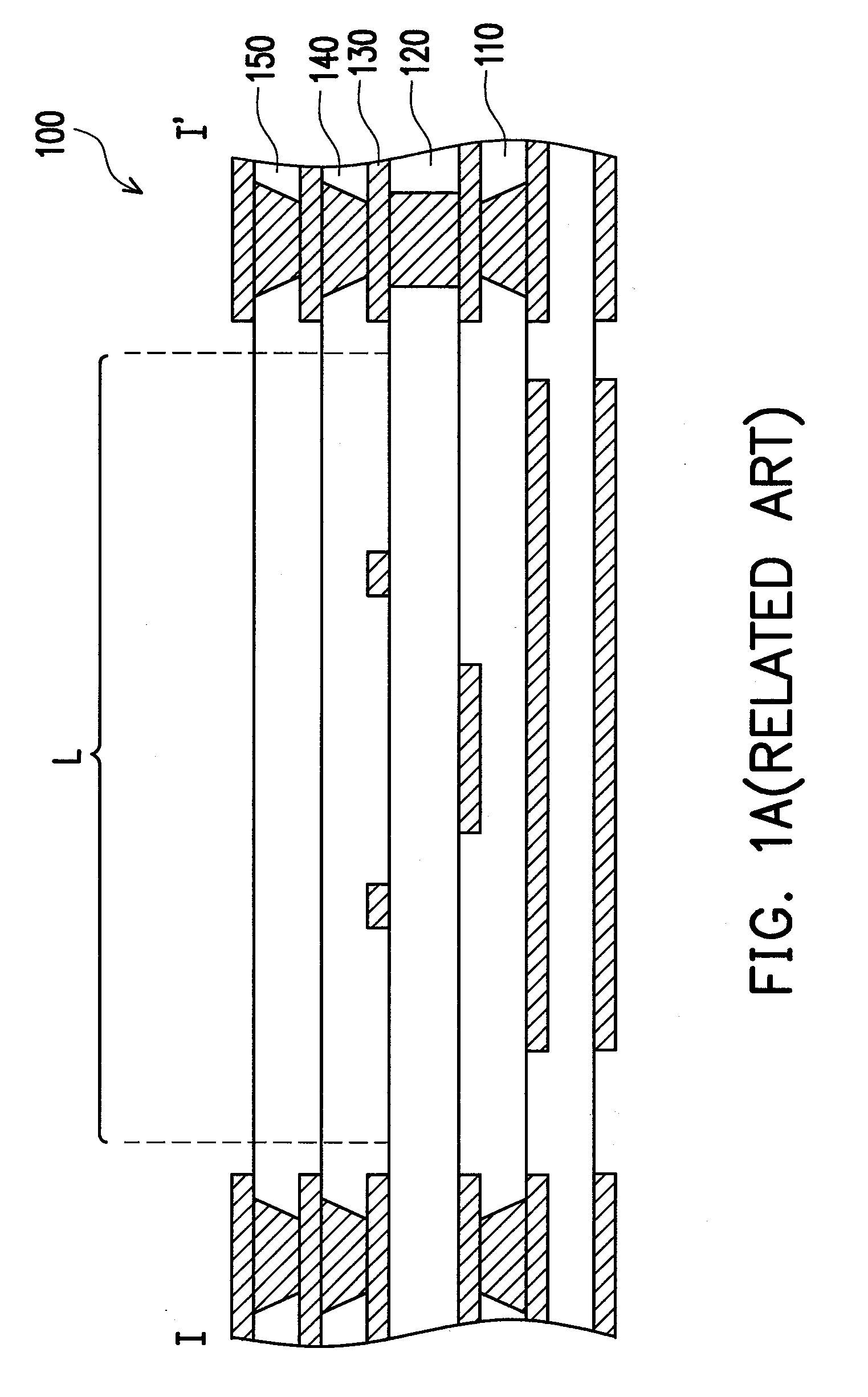
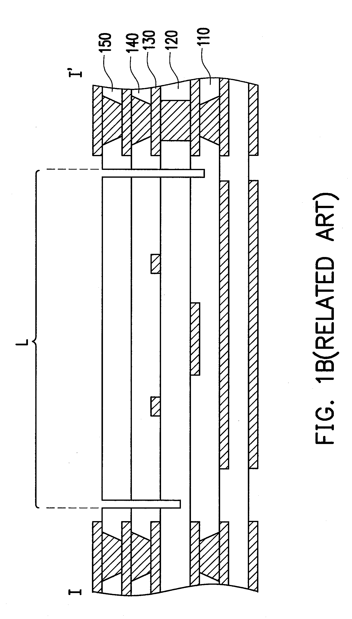
However, it is difficult to control the depth of the laser machining when the third dielectric layer 140 and the fourth dielectric layer 150 are removed through laser machining.

Method used


Image

  • Circuit board and manufacturing method thereof
  • Circuit board and manufacturing method thereof
  • Circuit board and manufacturing method thereof

Examples


Embodiment Construction

[0045]Reference will now be made in detail to the present preferred embodiments of the invention, examples of which are illustrated in the accompanying drawings. Wherever possible, the same reference numbers are used in the drawings and the description to refer to the same or like parts.

[0046]FIGS. 3A-3D′ and FIGS. 4A-4C are cross-sectional views illustrating a circuit board manufacturing process according to an embodiment of the present invention. FIG. 5 is a top view of a circuit layer and a second laser resistant structure of a substrate in FIGS. 3A-3C and FIGS. 4A-4C. FIG. 6 is a top view of a first laser resistant structure of the substrate in FIGS. 3A-3C and FIGS. 4A-4C.

[0047]It should be noted that the position of the line I-I′ in FIG. 5 is corresponding to the position of the line I-I′ in FIG. 6, and FIGS. 3A-3C are cross-sectional views illustrating a circuit board manufacturing process along the lines I-I′ in FIG. 5 and FIG. 6 according to an embodiment of the present inve...


PUM

PropertyMeasurementUnit
removing areaaaaaaaaaaa
areaaaaaaaaaaa
dielectricaaaaaaaaaa

Abstract

A circuit board having a removing area is provided. The circuit board includes a first dielectric layer, a first laser resistant structure disposed on the first dielectric layer and located at the periphery of the removing area, a second dielectric layer disposed on the first dielectric layer, a circuit layer disposed on the second dielectric layer, a second laser resistant structure disposed on the second dielectric layer and located at the periphery of the removing area, and a third dielectric layer disposed on the second dielectric layer. The second laser resistant structure is insulated from the circuit layer. There is a gap between the second laser resistant structure and the circuit layer, and the vertical projection of the gap on a first surface overlaps the first laser resistant structure. The third dielectric layer exposes the portion of the circuit layer within the removing area.

Description

CROSS-REFERENCE TO RELATED APPLICATION[0001]This application claims the priority benefit of Taiwan application serial no. 98111066, filed on Apr. 2, 2009. The entirety of the above-mentioned patent application is hereby incorporated by reference herein and made a part of this specification.BACKGROUND OF THE INVENTION[0002]1. Field of the Invention[0003]The present invention generally relates to a circuit board and a manufacturing method thereof, and more particularly, to a circuit board and a manufacturing method thereof with effective laser machining depth control.[0004]2. Description of Related Art[0005]Today's market demands electronic products to be designed small, slim, light, and highly portable. Accordingly, electronic parts in these electronic products have to be designed small and thin too. Thereby, a conventional technique for reducing the thickness of a portion of a circuit board is provided.[0006]FIGS. 1A-1C are cross-sectional views illustrating a conventional circuit b...

Claims


Application Information

Patent Timeline
Patent Type & Authority Applications(United States)
IPC IPC(8): H05K1/09H05K1/11H05K3/02B23K26/36H05K3/00H05K3/46
CPCH05K1/183H05K3/0035H05K3/06H05K3/4697H05K2201/09036H05K2201/09127Y10T29/49156H05K2203/0554H05K3/007H05K3/428H05K3/108H05K3/062Y10T29/49155H05K2201/09781
Inventor CHANG, CHEN-CHUAN
Owner UNIMICRON TECH CORP
Learn More