Organic light-emitting display panel, display device, and manufacturing method for organic light-emitting display panel

A light-emitting display and organic technology, applied in semiconductor/solid-state device manufacturing, semiconductor devices, electrical components, etc., can solve the problems of reduced reliability of organic light-emitting display panel packaging, formation of foreign objects, damage to retaining walls, etc.

Active Publication Date: 2018-03-27
SHANGHAI TIANMA MICRO ELECTRONICS CO LTD
View PDF3 Cites 36 Cited by
  • Summary
  • Abstract
  • Description
  • Claims
  • Application Information

AI Technical Summary

Problems solved by technology

[0003] In the production process of organic light-emitting display panels, structures such as light-emitting functional layers are often formed by evaporation in the display area through masks, and the retaining walls that are in contact with the masks during the evaporation process are often made of organic materials. , the friction generated between the mask and the retaining wall is likely to cause the organic material to fall off from the retaining wall. On the one hand, the detached organic material forms foreign matter in the organic light-emitting display panel; Lead to reduced packaging reliability of organic light-emitting display panels

Method used


Image

  • Organic light-emitting display panel, display device, and manufacturing method for organic light-emitting display panel
  • Organic light-emitting display panel, display device, and manufacturing method for organic light-emitting display panel
  • Organic light-emitting display panel, display device, and manufacturing method for organic light-emitting display panel

Examples


Embodiment Construction

[0029] The present invention will be further described in detail below in conjunction with the accompanying drawings and embodiments. It should be understood that the specific embodiments described here are only used to explain the present invention, but not to limit the present invention. In addition, it should be noted that, for the convenience of description, only some structures related to the present invention are shown in the drawings but not all structures.

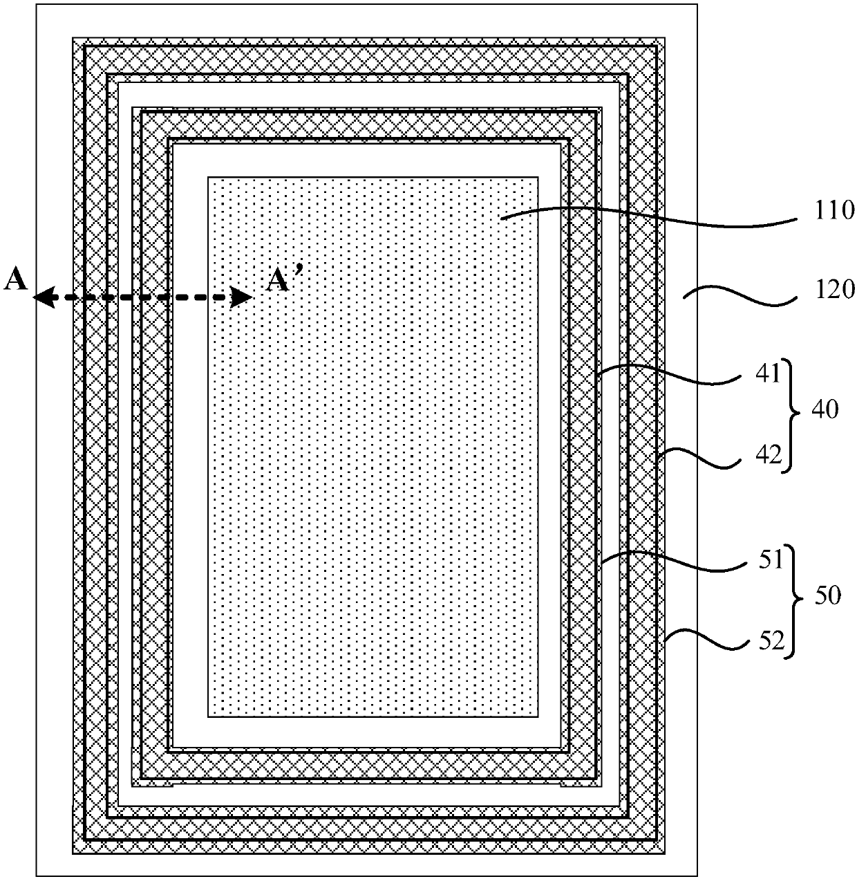
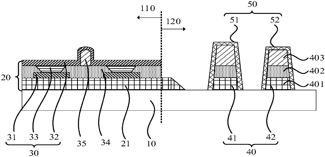
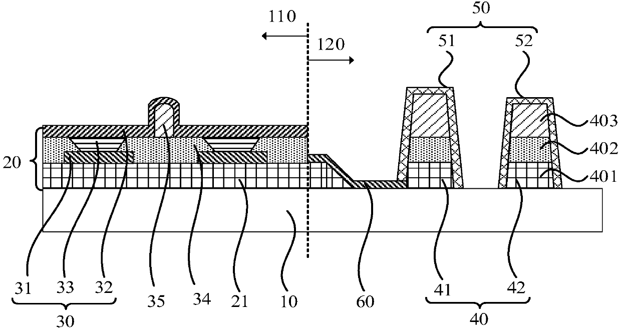
[0030] figure 1 It is a schematic top view structure diagram of an organic light emitting display panel provided by an embodiment of the present invention, figure 2 for along figure 1 Schematic diagram of the cross-sectional structure in the direction of AA', combined with figure 1 and figure 2 As shown, the organic light emitting display panel includes: a substrate 10 , an organic light emitting component 20 , at least one barrier wall 40 and at least one protective metal layer 50 . The substrate 10 include...


PUM


Abstract

The invention provides an organic light-emitting display panel, a display device, and a manufacturing method for the organic light-emitting display panel. The organic light-emitting display panel comprises a substrate which comprises a display region and a non-display region, wherein the non-display region surrounds the display region; an organic light-emitting part which is located in the displayregion, and is disposed at a first side of the substrate; at least one retaining wall which is disposed in the non-display region and surrounds the organic light-emitting part; and at least one protection metal layer which is located in the non-display region and is located at one side, far from the substrate, of the retaining wall, wherein the vertical projection of the retaining wall on the substrate is located in the vertical projection of the protection metal layer on the substrate. The foreign matters formed in the organic light-emitting display panel are eliminated, and the packaging reliability of the organic light-emitting display panel is improved.

Description

technical field [0001] The present invention relates to the field of display technology, in particular to an organic light emitting display panel, a display device and a manufacturing method thereof. Background technique [0002] OLED (Organic Light Emitting Diode, Organic Light Emitting Diode) display is a self-luminous display. Compared with LCD (Liquid Crystal Display, Liquid Crystal Display), OLED display does not require a backlight source, so OLED display is thinner and lighter. In addition, OLED display is also Due to the advantages of high brightness, low power consumption, wide viewing angle, high response speed, and wide operating temperature range, it is increasingly used in various high-performance display fields. [0003] In the production process of organic light-emitting display panels, structures such as light-emitting functional layers are often formed by evaporation in the display area through masks, and the retaining walls that are in contact with the mask...

Claims


Application Information

Patent Timeline
Patent Type & Authority Applications(China)
IPC IPC(8): H01L27/32H01L51/52H01L51/56
CPCH10K59/88H10K50/8428H10K71/00
Inventor 姜文鑫李针英
Owner SHANGHAI TIANMA MICRO ELECTRONICS CO LTD
Why Eureka
Try Eureka