
Touch display device and method for manufacturing the same

Active Publication Date: 2015-12-31
WUHAN TIANMA MICRO ELECTRONICS CO LTD +1
View PDF2 Cites 37 Cited by
  • Summary
  • Abstract
  • Description
  • Claims
  • Application Information

AI Technical Summary

Benefits of technology

The touch display device and manufacturing method in this patent allow for signals to be sent between two substrates, which results in a simpler fabrication process, higher yield, narrower borders, and a thinner display.

Problems solved by technology

With the progress of technology and the increased requirements of customers, many disadvantages of the above structure of the touch display device are obvious.
Specifically, for the first scheme, the process capability of the conductive golden ball is poor, and there are many problems, for example, in coating the golden balls and in metallic contact between the golden balls and the substrates, thereby affecting product yield.
Furthermore, in the case that the conductive golden balls are used as the medium for transmitting the signal between the upper substrate and the lower substrate, borders of the touch display device may not be narrowed due to poor alignment accuracy.
Additionally, a distance between the upper substrate and the lower substrate may not be reduced due to the usage of the conductive golden balls.
The second scheme may inevitably increase the cost due to the addition of the FPCs.

Method used


Image

  • Touch display device and method for manufacturing the same
  • Touch display device and method for manufacturing the same
  • Touch display device and method for manufacturing the same

Examples


Embodiment Construction

[0030]In the following, technical solutions according to embodiments of the disclosure are described clearly and completely in conjunction with the accompanying drawings. Apparently, the described embodiments are merely a part of rather than all of the embodiments of the disclosure. Any other embodiments obtained by those skilled in the art based on the embodiments in the disclosure without any creative works will fall within the scope of the disclosure.

[0031]The term “vertical”, as used herein, means substantially perpendicular to the surface of a substrate. Propositions, such as “on”, “side”, “above”, “below” are defined with respect to the conventional surface of a substrate regardless of the orientation of the substrate. The term “upwardly” refers to a direction from the bottom to the top.

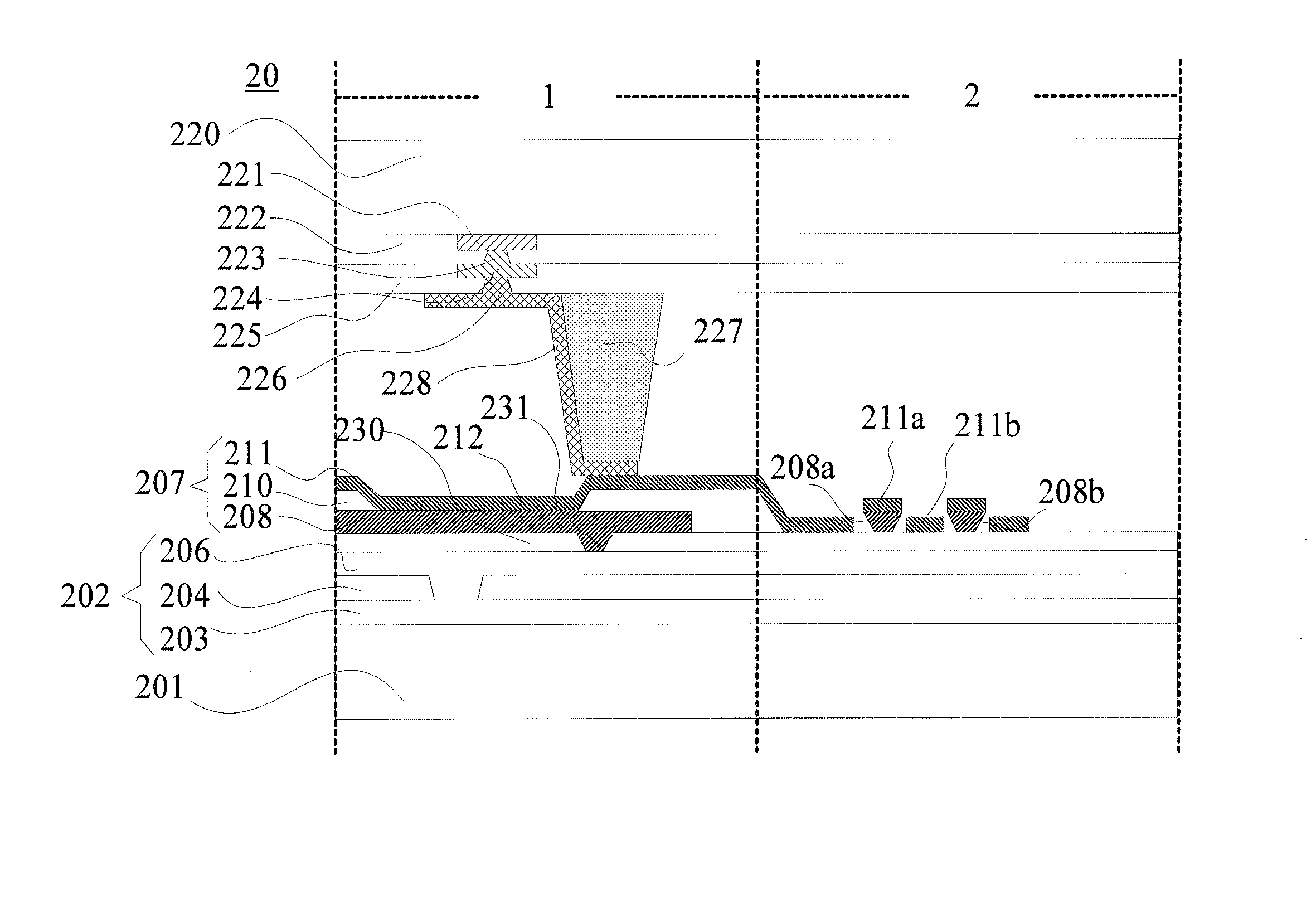
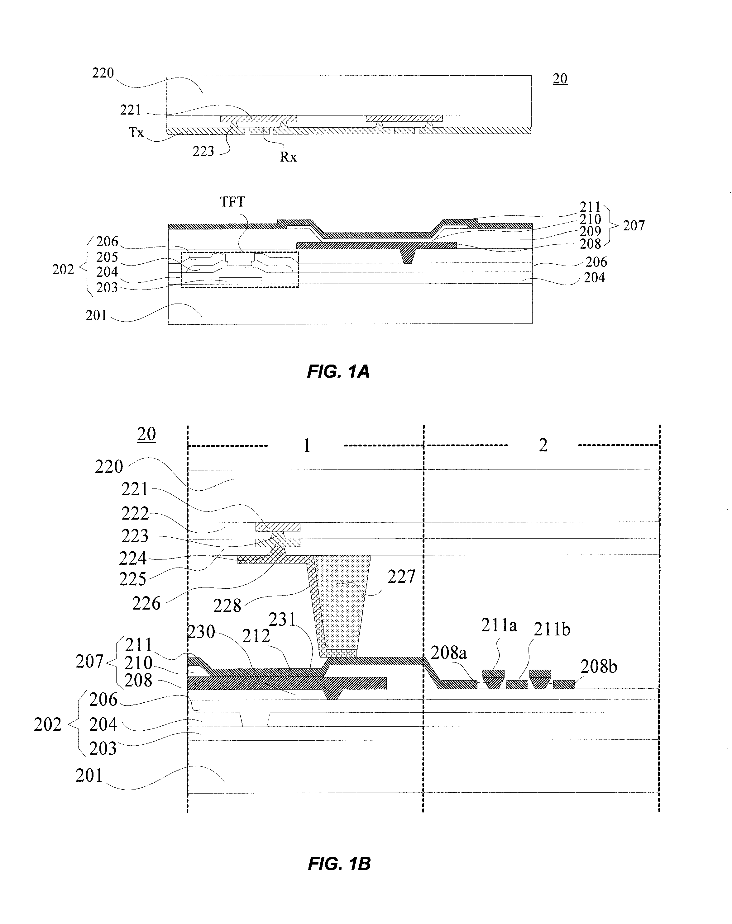
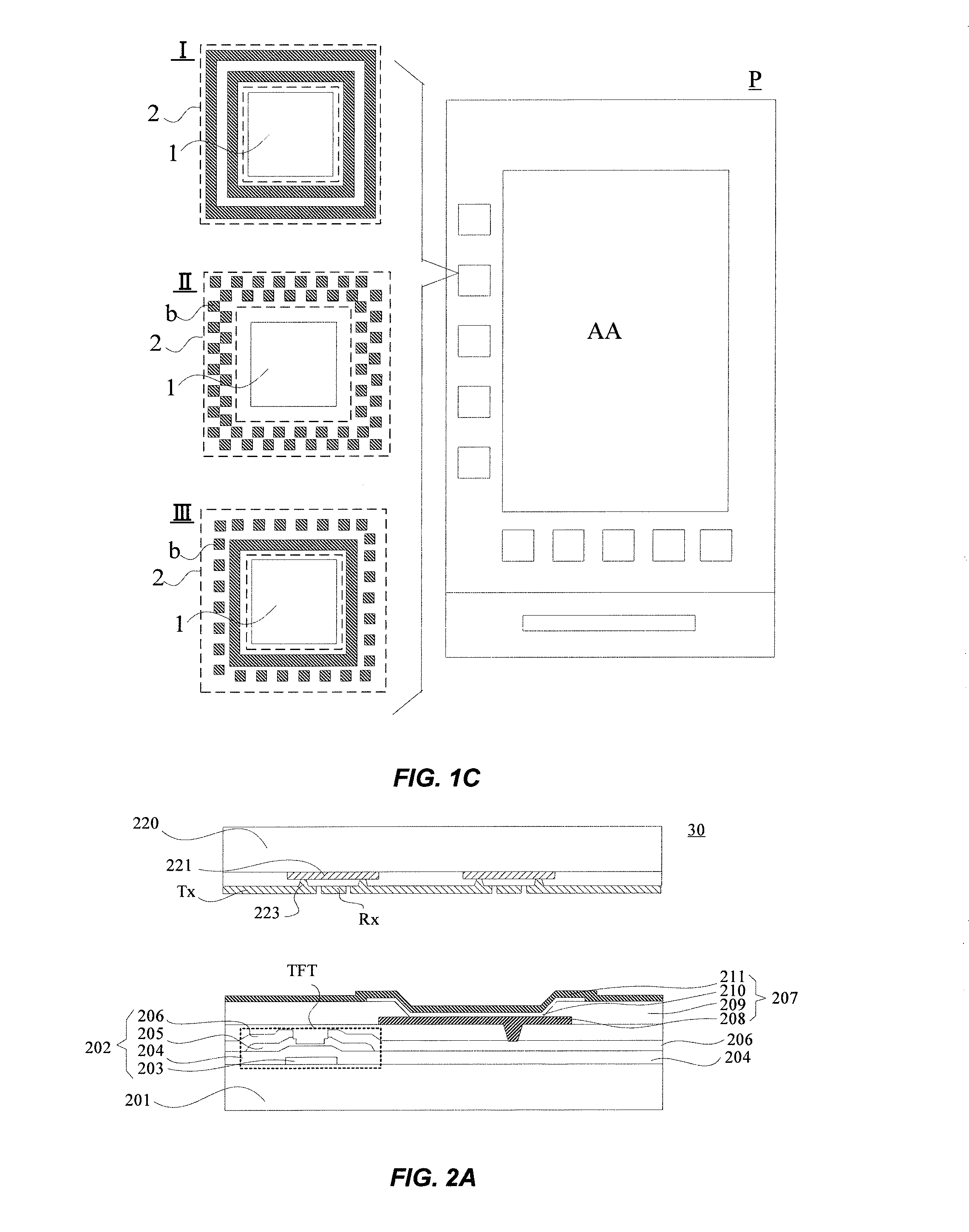
[0032]FIG. 1A and FIG. 1B are respective sectional views of a display region and a periphery region of a touch display device 20 according to an embodiment of the disclosure.

[0033]As shown in F...


PUM


Abstract

A touch display device and a method for manufacturing the same are provided. The touch display device includes a first substrate, a second substrate disposed opposite to the first substrate, and at least one touch signal transmission unit. The touch signal transmission unit includes: a first conductive layer located above a side of the first substrate facing the second substrate; a second conductive layer located above a side of the second substrate facing the first substrate; a touch signal transmission layer, located between the second conductive layer and the second substrate and electrically connected to the first conductive layer via the second conductive layer; and a spacer located between the first substrate and the second substrate, where a vertical projection of the spacer onto the first substrate at least partially overlaps vertical projections of the first conductive layer and the second conductive layer onto the first substrate.

Description

CROSS-REFERENCES TO RELATED APPLICATIONS[0001]This application claims the benefit of priority to Chinese Patent Application No. 201410309292.7, filed with the Chinese Patent Office on Jun. 30, 2014 and entitled “TOUCH DISPLAY DEVICE AND METHOD FOR MANUFACTURING THE SAME”, the content of which is incorporated herein by reference in its entirety.FIELD[0002]The disclosure relates to touch control technologies, and in particular to a touch display device and a method for manufacturing the same.BACKGROUND OF THE INVENTION[0003]With the rapid development of display technology, touch screen panels have become popular in people's life. At present, a conventional in-cell capacitive touch display is achieved by adding touch scanning lines and touch sensing lines on a conventional Thin Film Transistor (TFT) array substrate. That is, two layers of strip electrodes are formed on a surface of the TFT array substrate, the strip electrodes in one layer intersecting with the strip electrodes in the ...

Claims


Application Information

Patent Timeline
IPC IPC(8): H01L27/32H01L51/56
CPCG06F3/047H01L27/323H01L27/3246G06F3/0412G06F3/0416G06F3/044G06F2203/04103G06F2203/04111G06F3/04164G06F3/0443H10K59/40H10K59/122
Inventor SU, CONGYI
Owner WUHAN TIANMA MICRO ELECTRONICS CO LTD
Learn More