Non-Volatile Semiconductor Memory Devices Having Charge Trap Layers Between Word Lines and Active Regions Thereof

a semiconductor memory and non-volatile technology, applied in the field of semiconductor memory devices, can solve problems such as the loss of stored data of volatile semiconductor memory devices, and achieve the effect of improving reliability and/or performan

Active Publication Date: 2010-10-07
SAMSUNG ELECTRONICS CO LTD
View PDF11 Cites 38 Cited by
  • Summary
  • Abstract
  • Description
  • Claims
  • Application Information

AI Technical Summary

Benefits of technology

[0005]Embodiments of the present invention provide non-volatile semiconductor memory devices that may exhibit enhanced reliability and / or performance.

Problems solved by technology

Volatile semiconductor memory devices lose stored data when a power supply to the memory device is interrupted.
The height of the floating gate, however, may act as an impediment to further scaling down the size of a highly integrated flash memory device.

Method used


Image

  • Non-Volatile Semiconductor Memory Devices Having Charge Trap Layers Between Word Lines and Active Regions Thereof
  • Non-Volatile Semiconductor Memory Devices Having Charge Trap Layers Between Word Lines and Active Regions Thereof
  • Non-Volatile Semiconductor Memory Devices Having Charge Trap Layers Between Word Lines and Active Regions Thereof

Examples


Embodiment Construction

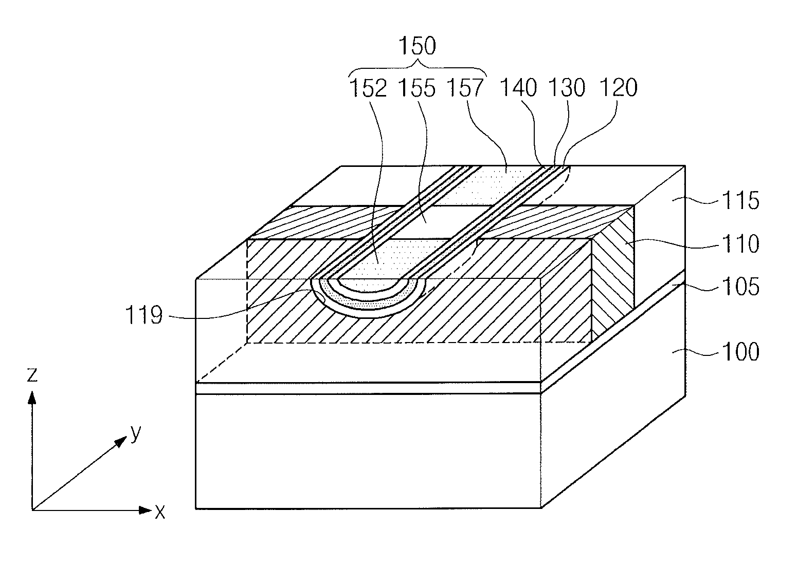
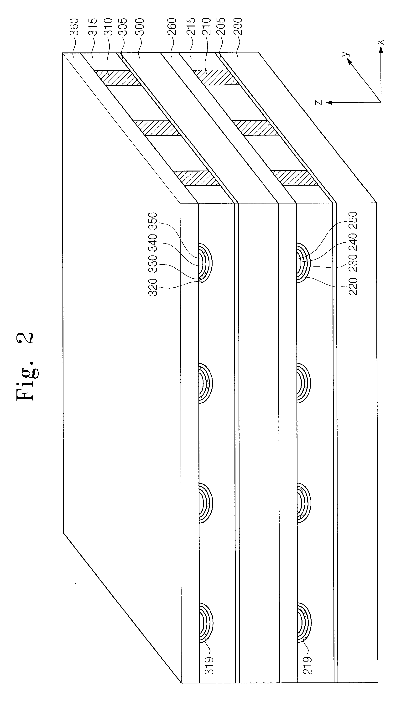
[0019]Exemplary embodiments of the present invention will be described below in more detail with reference to the accompanying drawings. The present invention may, however, be embodied in different forms and should not be construed as limited to the embodiments set forth herein. Rather, these embodiments are provided so that this disclosure will be thorough and complete, and will fully convey the scope of the invention to those skilled in the art. Like numbers refer to like elements throughout.

[0020]It will be understood that, although the terms first, second, etc. may be used herein to describe various elements, these elements should not be limited by these terms. These terms are only used to distinguish one element from another. As used herein, the term “and / or” includes any and all combinations of one or more of the associated listed items.

[0021]It will be understood that when an element such as a layer, region or substrate is referred to as being “on” or extending “onto” another...


PUM


Abstract

A non-volatile memory device includes: word line disposed on a substrate; an active region crossing over the word line; and a charge trap layer that is between the word line and the active region.

Description

CROSS-REFERENCE TO RELATED APPLICATION[0001]This U.S. non-provisional patent application claims priority under 35 U.S.C. §119 to Korean Patent Application No. 10-2009-0029588, filed on Apr. 6, 2009, the entire contents of which are incorporated by reference herein as if set forth in its entirety.BACKGROUND[0002]The present disclosure herein relates to semiconductor memory devices and, more particularly, to non-volatile semiconductor memory devices.[0003]Semiconductor memory devices may generally be classified as volatile or non-volatile memory devices. Volatile semiconductor memory devices lose stored data when a power supply to the memory device is interrupted. Non-volatile semiconductor memory devices can retain data even when the power supply to the device is interrupted. Flash memory devices are one well known type of non-volatile semiconductor memory that may be highly integrated and which may have the advantages of both an EPROM (Erasable Programmable Read Only Memory) device ...

Claims


Application Information

Patent Timeline
Patent Type & Authority Applications(United States)
IPC IPC(8): H01L29/792
CPCH01L21/28282H01L27/11568H01L29/792H01L29/66833H01L27/11578H01L29/40117H10B43/20H10B43/30H10B20/40
Inventor NAKANISHI, TOSHIROPARK, CHANJINCHOI, SIYOUNGKOO, BONYOUNG
Owner SAMSUNG ELECTRONICS CO LTD
Why Eureka
Try Eureka