

Thermal stress reduction
a technology of thermal stress and reduction of stress, which is applied in the direction of semiconductor devices, semiconductor/solid-state device details, capacitors, etc., can solve the problems of warping and less manageable wafers, high cost, and breakage of wafers
- Summary
- Abstract
- Description
- Claims
- Application Information
AI Technical Summary
Benefits of technology
Problems solved by technology
Method used
Image

Examples
Embodiment Construction
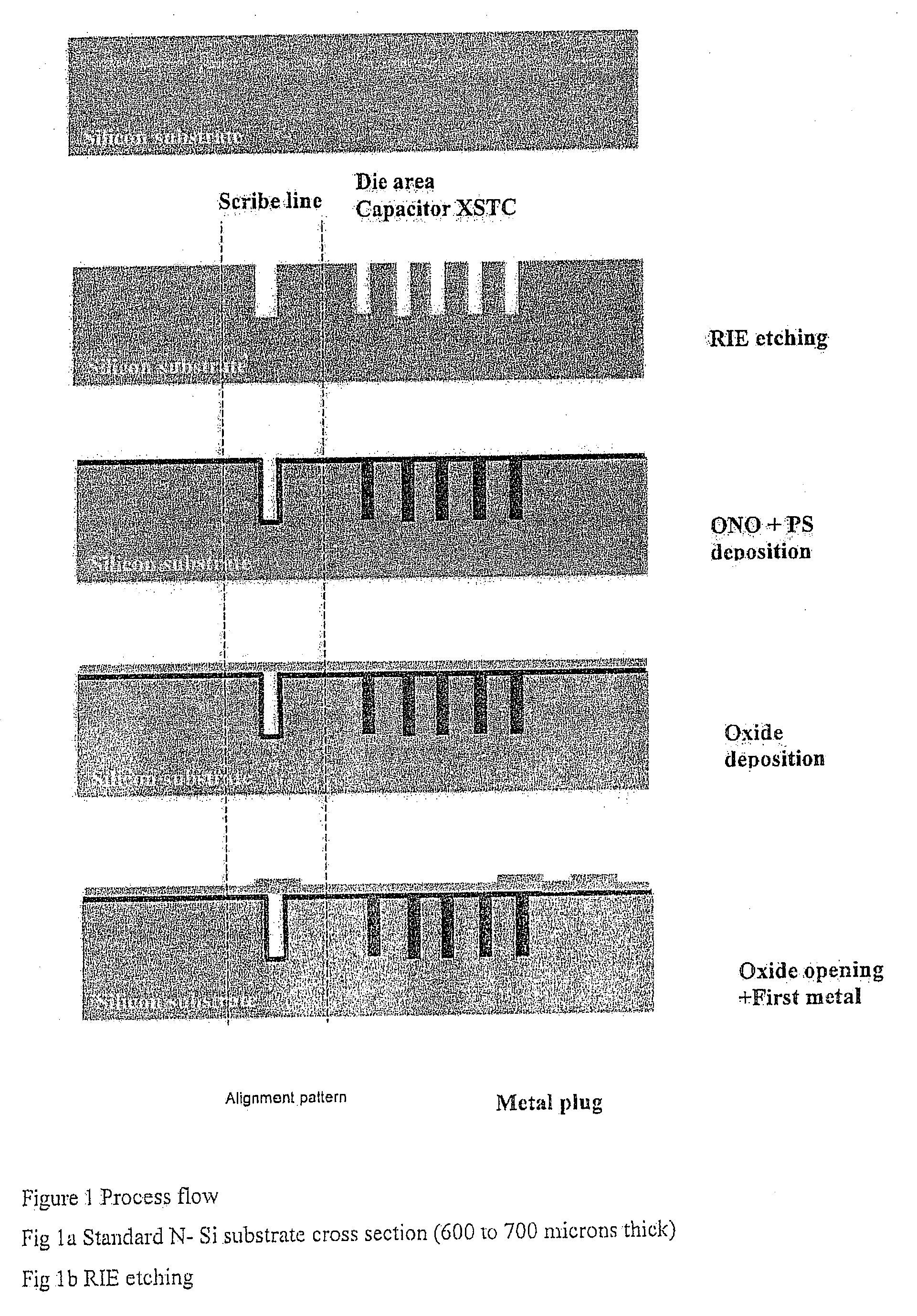
[0016]In a first embodiment the invention relates to a method for thermal stress reduction on a wafer, comprising the steps of:
[0017]providing a wafer with an alignment pattern and saw lanes between adjacent dies,
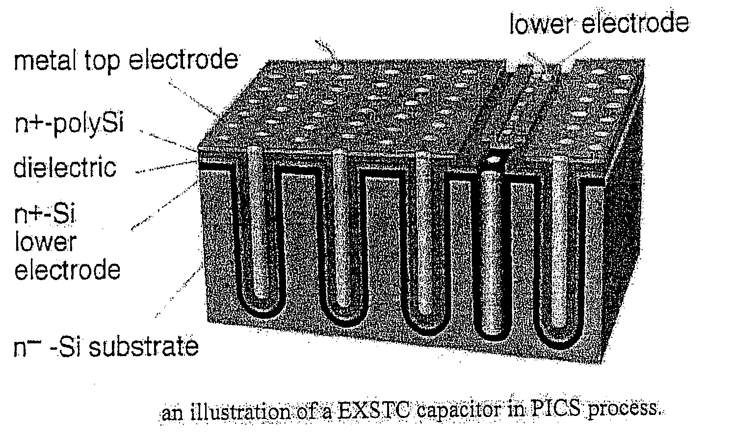
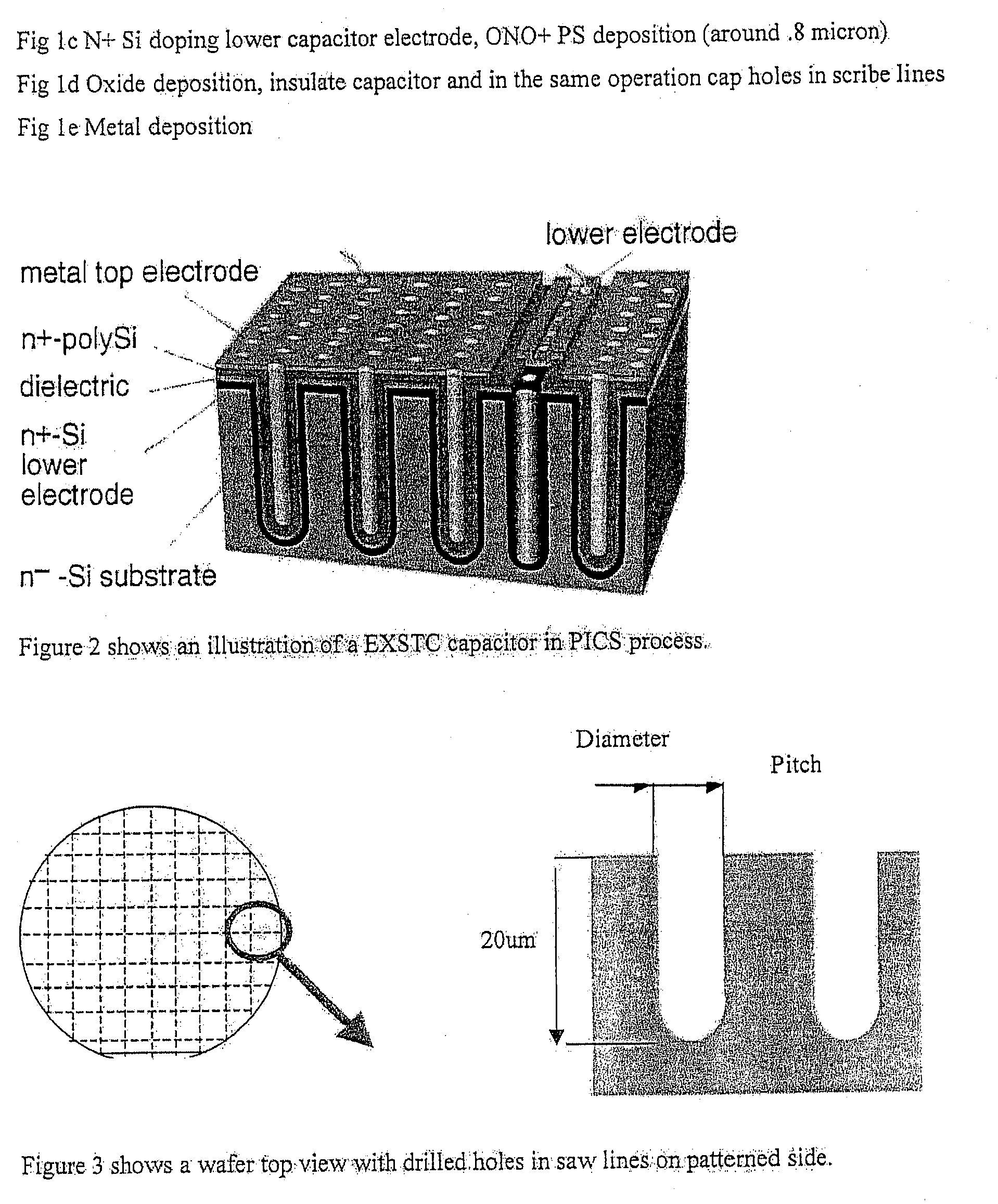
[0018]forming thin holes within the silicon substrate, which holes create a dotted groove in the saw lanes, wherein no second layer on an opposing side of the wafer is formed.
[0019]In order to be able to define dies on a wafer, an alignment pattern for lithographic equipment needs to be present.
[0020]Whenever the term “saw lanes” is used, it also refers to scribe lanes or scribe lines.
[0021]Further, it is not necessary that the saw lanes have already been physically defined on the wafer. Actually, and preferably, the saw lanes may also be virtually present, that is, the holes which are formed by the present method, are formed at locations, where in subsequent process steps the saw lanes are formed. As such, the holes would be present “underneath” saw lanes, that is in a ver...
PUM
 Abstract
Description
Claims
Application Information