Defect inspecting method, defect inspecting apparatus, and storage medium storing defect inspection program

a defect inspection and defect technology, applied in the field of defect inspection methods, can solve problems such as adverse effects on productivity, and achieve the effects of facilitating rapid analysis of the cause of defects, presenting deterioration in productivity, and identifying quickly

Active Publication Date: 2010-10-21
TOKYO ELECTRON LTD
View PDF7 Cites 25 Cited by
  • Summary
  • Abstract
  • Description
  • Claims
  • Application Information

AI Technical Summary

Benefits of technology

[0013]According to the present invention, a film having the defect can be identified rapidly. This facilitates analysis of the cause of the defect rapidly, and presents deterioration in productivity.

Problems solved by technology

Thus, it takes a lot of time to judge whether the defect is critical or not and to find out a cause of the defect, resulting in serious adverse affect on the productivity.

Method used


Image

  • Defect inspecting method, defect inspecting apparatus, and storage medium storing defect inspection program
  • Defect inspecting method, defect inspecting apparatus, and storage medium storing defect inspection program
  • Defect inspecting method, defect inspecting apparatus, and storage medium storing defect inspection program

Examples


Embodiment Construction

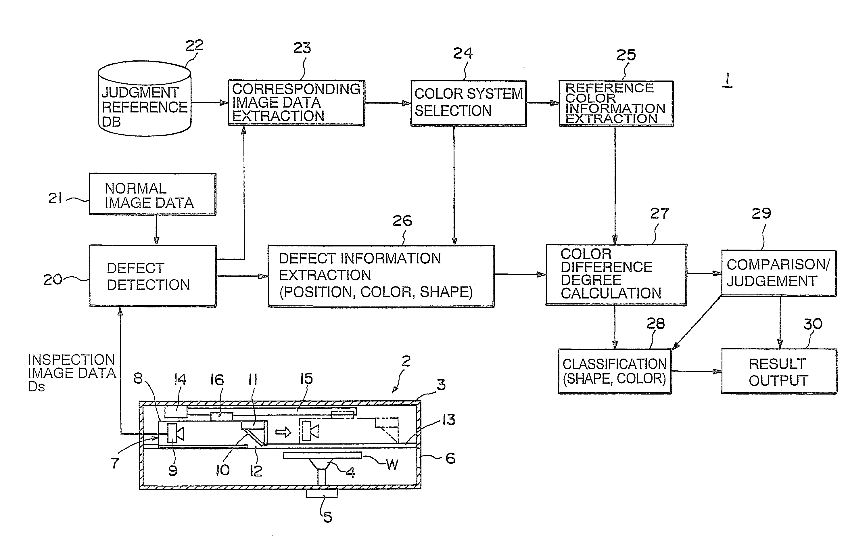
[0021]An embodiment of the present invention will be described below with reference to the accompanying drawings. In the present invention, a semiconductor wafer (also referred to simply as “wafer”) is an inspection target. The present invention can be suitably employed in an inspecting step before an exposure step or the like, in a photolithographic process included in a semiconductor device manufacturing.

[0022]FIG. 1 is a block diagram showing the overall structure of a defect inspecting apparatus 1 used in this embodiment. The defect inspecting apparatus 1 is particularly configured to detect a defect in a plurality of films (e.g., a base film, a resist film, and a top coat film), which are sequentially stacked on layers on the surface of a wafer W by a photolithographic process, and specifically configured to detect a defect which occurs during formation of the films (e.g., uncoated portion).

[0023]In FIG. 1, the defect inspecting apparatus 1 includes an image data acquiring unit...


PUM


Abstract

There is provided a database storing reference data including a plurality of reference image data, which are obtained by imaging reference substrates, respectively, wherein each of the reference substrates lacks only one of the films of different kinds but includes remainder of the films of different kinds, and wherein in the reference substrates the lacking films are different from each other, and wherein the plurality of reference image data is classified into categories according to the kinds of the films. Difference degrees between color information of a defect area extracted from an image data of an inspection target substrate and color information of corresponding areas of the reference substrates are calculated. Based on the difference degree, the defective film is identified.

Description

FIELD OF THE INVENTION[0001]The present invention relates to a defect inspecting method, a defect inspecting apparatus, and a storage medium storing a defect inspecting program, for inspecting a defect on a substrate to be processed such as a semiconductor wafer.BACKGROUND ART[0002]A photolithographic process in a manufacture of a semiconductor device includes a resist coating step that forms a resist film on the surface of a semiconductor wafer, an exposing step that exposes the resist-coated semiconductor wafer with a predetermined pattern, and a developing step that develops the exposed resist. The substrate, which has been subjected to the series of process steps, is then subjected to a macro defect inspection in which the substrate is inspected by an inspecting apparatus that inspects whether or not a predetermined film has been suitably formed on the surface of the substrate, whether or not the substrate has been suitably exposed, and whether or not there are damages or partic...

Claims


Application Information

Patent Timeline
Patent Type & Authority Applications(United States)
IPC IPC(8): G06K9/00G06V10/56
CPCG06K9/4652G06T2207/30148G06T2207/10024G06T7/001G06V10/56
Inventor IWANAGA, SHUJI
Owner TOKYO ELECTRON LTD
Why Eureka
Try Eureka