Display Device
- Summary
- Abstract
- Description
- Claims
- Application Information
AI Technical Summary
Benefits of technology
Problems solved by technology
Method used
Image
Examples
first embodiment
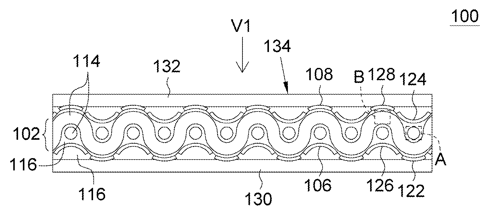
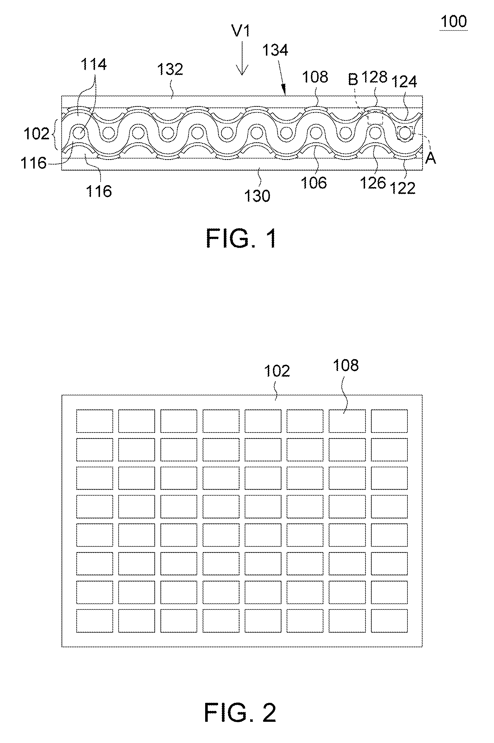
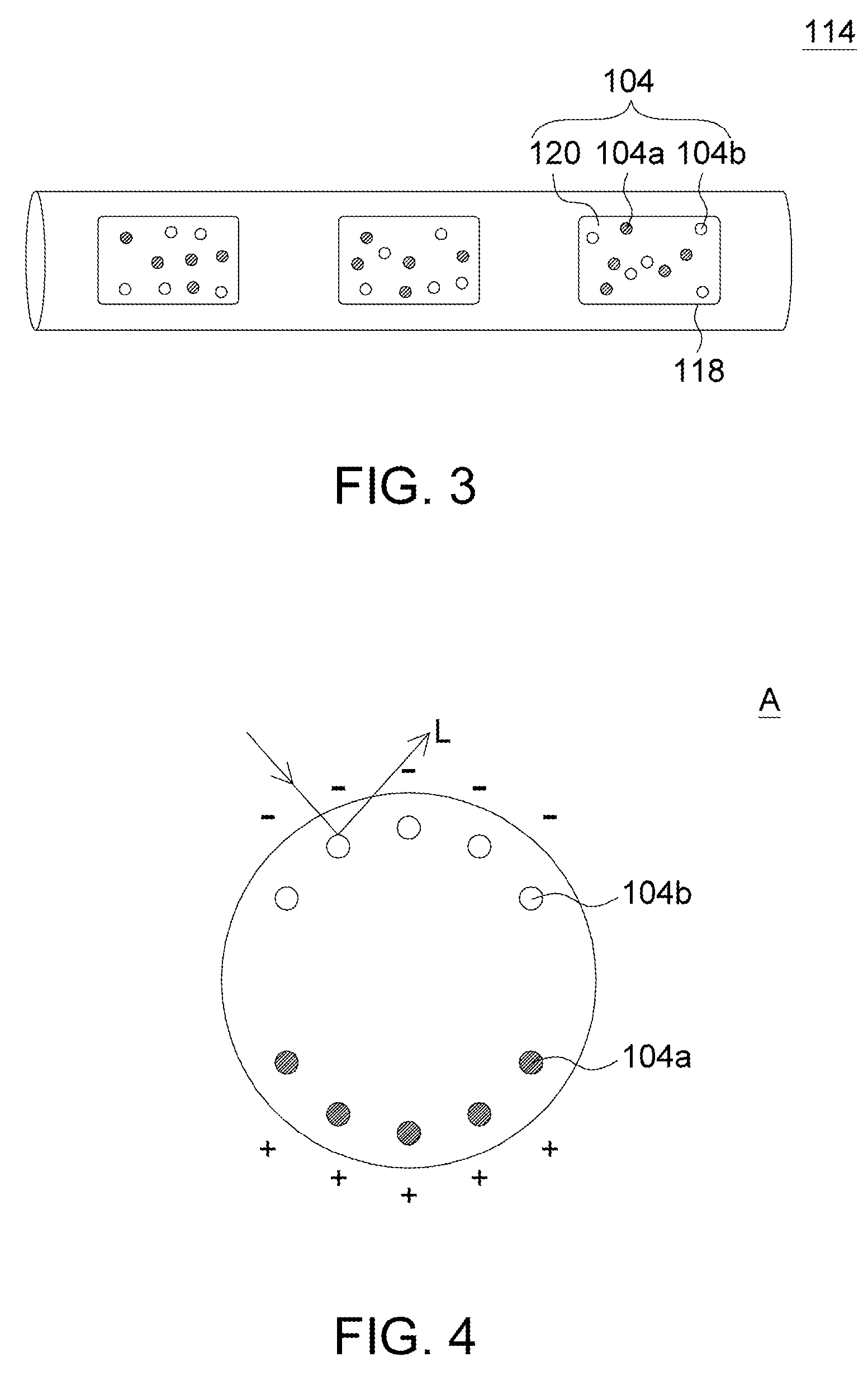
[0018]Referring to FIG. 1, FIG. 2 and FIG. 3. FIG. 1 shows a display device according to a first embodiment of the invention. FIG. 2 shows a matrix electrode layer viewed along direction V1 of FIG. 1. FIG. 3 shows an enlargement of a single fiber of FIG. 1. As indicated in FIG. 1, the display device 100 includes a fiber layer 102, a first electrode layer 106, a second electrode layer 108, a dielectric layer 116, a first substrate 130, a second substrate 132, a driving module (not illustrated) and a display surface 134. The second substrate 132 is opposite to the first substrate 130. The first substrate 130 and the second substrate 132 are transparent substrates.
[0019]The fiber layer 102 is disposed between the first substrate 130 and the second substrate 132 and includes a plurality of fibers 114 and a display medium 104 (illustrated in FIG. 3) and a plurality of capsules 118 (illustrated in FIG. 3), wherein the display medium 104 is disposed within the fibers 114.
[0020]The first el...
second embodiment
[0032]Referring to FIG. 7 which shows a display device according to a second embodiment of the invention. As for the similarities between the present embodiment of the invention and the first embodiment, the same designations are used and are not repeated here. The display device 300 of the second embodiment differs with the display device 100 of the first embodiment in that the display device 300 is a color display device.
[0033]Furthermore, the display device 300 includes a color filter (color filter) 304, and the first electrode layer of the display device 300 is an active element array structure layer 302, such as thin film transistor (TFT). The color filter 304 is disposed between the fiber layer 102 and the second substrate 306, and the active element array structure layer 302 is disposed between the fiber layer 102 and the first substrate 130.
[0034]Moreover, the second electrode layer 308 of the present embodiment of the invention is a common electrode driven by the driving mo...
PUM
 Abstract
Description
Claims
Application Information


