Electronic component and method for producing the same

a technology of electronic components and components, applied in the direction of electrical apparatus construction details, non-metallic protective coating applications, lighting and heating apparatuses, etc., can solve the problems of large increase in costs, inability to mount elements with such a small pitch, and failure to prevent the failure of electronic components. , the effect of thin electronic components

Active Publication Date: 2005-08-25
MURATA MFG CO LTD
View PDF7 Cites 0 Cited by
  • Summary
  • Abstract
  • Description
  • Claims
  • Application Information

AI Technical Summary

Benefits of technology

[0016] With the surface of the base to which the elements are mounted facing downward, the elements are immersed in an insulating resilient material, such as a liquid resin or a semi-solid resin. After the insulating resilient material has hardened, the hardened insulating resilient material is removed, resulting in the formation of the cover. The method for producing an electronic component prevents entry of the resin into through holes in the base, and thus, prevents conduction failure of the electronic component.
[0017] In addition, a thinner electronic component can be provided by embedding the elements in the cover.

Problems solved by technology

However, when mounting the resin cover to the base whose surface to which the elements are mounted includes through holes, if the resin enters the openings of the through holes, conduction failure occurs.
Therefore, in a small electronic component, elements cannot be mounted with such a small pitch.
Therefore, when each of the through holes is covered with a very small metallic plate as in the aforementioned document, costs are considerably increased.
In addition, when the very small metallic plates are disposed at predetermined locations, gaps may be formed between the metallic plates and the openings of the through holes.
If these gaps are formed, resin is not prevented from entering the through holes, and as a result, quality control problems are not entirely eliminated when mass production is considered.

Method used


Image

  • Electronic component and method for producing the same
  • Electronic component and method for producing the same
  • Electronic component and method for producing the same

Examples


first preferred embodiment

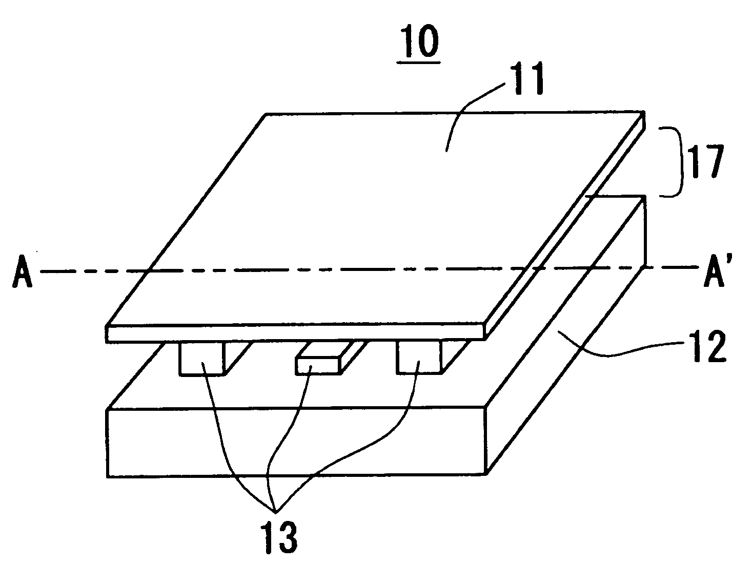
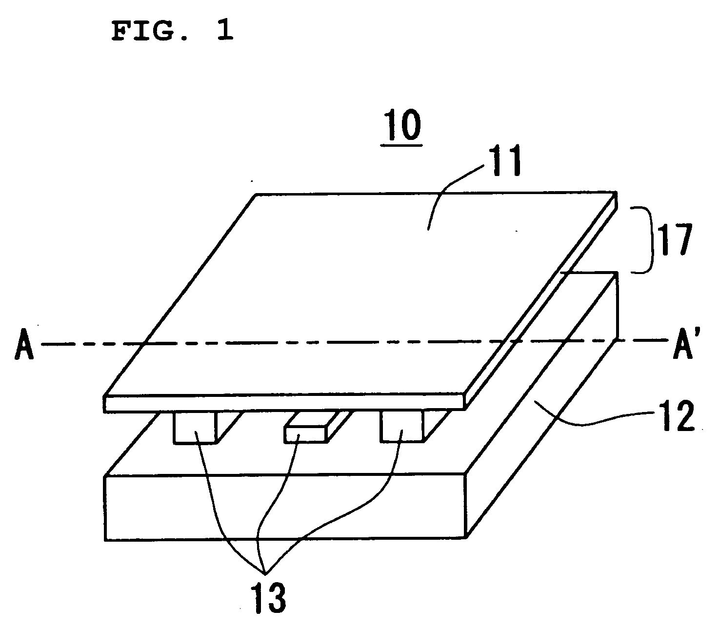
[0027]FIG. 1 is an external perspective view of a multi-layer substrate 10 in accordance with a first preferred embodiment of the present invention. In the multi-layer substrate 10, elements 13 are mounted to a base 12, and a cover 11 is supported by some of the elements 13 and covers the elements 13.

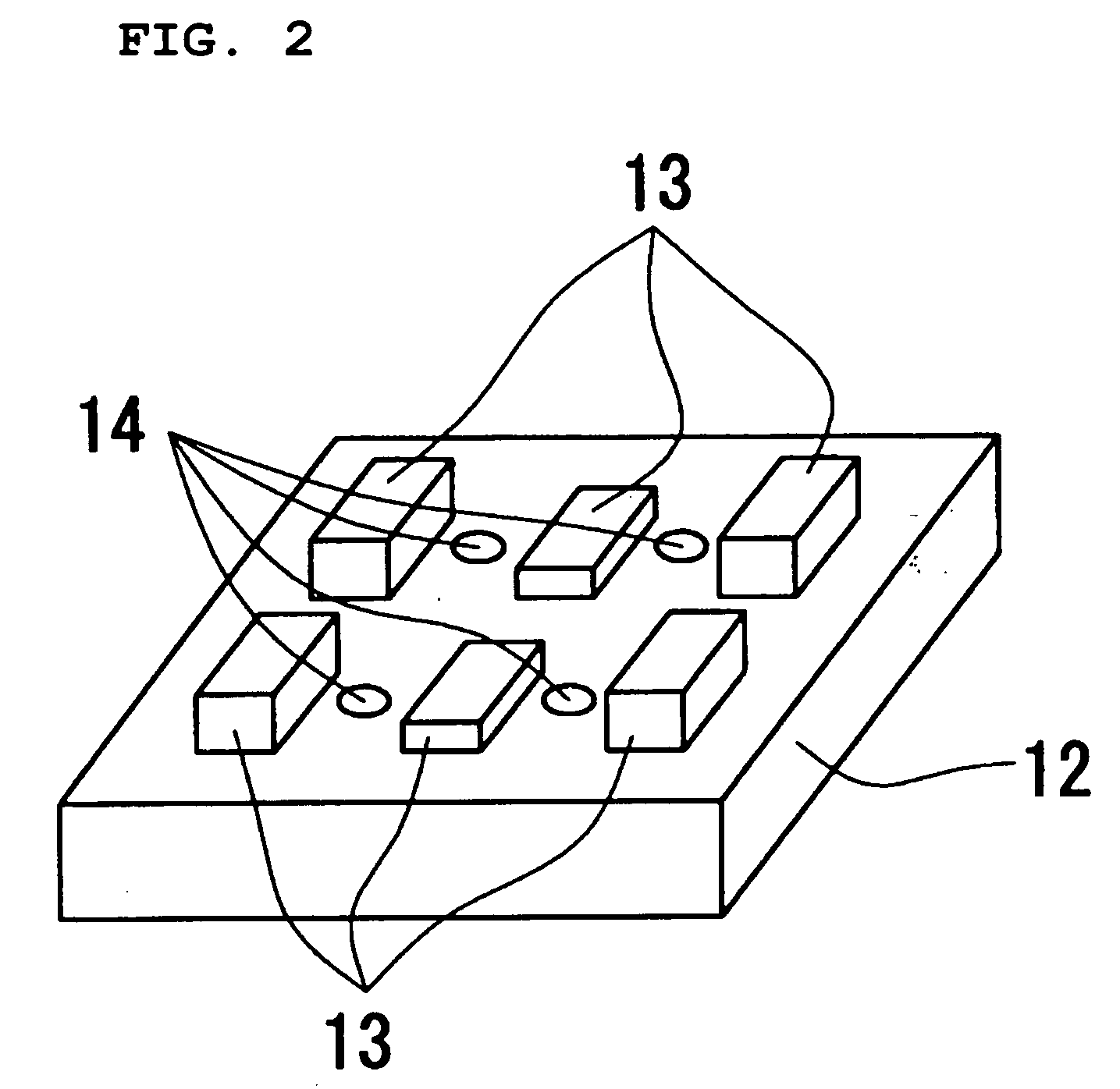
[0028] The base 12 is formed, for example, in the following manner. Wiring circuits are formed on a desired number of ceramic sheets, and the ceramic sheets are laminated. Thereafter, through holes filled with conductive paste for electrically connecting the ceramic sheets are formed, after which the resulting structure is fired. Then, the wiring circuit disposed on a principal surface of the base is coated, and the elements 13 are soldered and mounted to the wiring circuit. FIG. 2 is a perspective view of an element surface of the base 12 without the cover 11 shown in FIG. 1. The elements 13 are mounted to the element surface of the base 12, and through holes 14 are disposed in the el...

second preferred embodiment

[0033]FIGS. 4A and 4B and FIGS. 4C to 4E are, respectively, external perspective views and sectional views for illustrating a method for producing a multi-layer substrate in accordance with a second preferred embodiment of the present invention. Elements shown in FIGS. 4A to 4E that correspond to those shown in FIG. 1 are given the same reference numerals, and descriptions thereof are omitted.

[0034] First, as shown in FIG. 4A, a base 12 having elements 13 mounted thereon, is provided.

[0035] Next, a tray (container) 32 is filled with a predetermined amount of liquid insulating material, such as epoxy resin. This resin 31 may be a liquid or a semi-solid and its viscosity is not particularly limited as long as the elements can be immersed in the resin 31. The tray 32 is also previously coated with a separation agent such that the hardened resin 31 can be easily removed from the tray 32.

[0036] Next, as shown in FIG. 4B, with an element surface of the base 12 to which the elements 13 ...

third preferred embodiment

[0038]FIG. 5A is an external perspective view and FIGS. 5B to 5D are sectional views for illustrating a method for producing a multi-layer substrate in accordance with a third preferred embodiment of the present invention. In FIGS. 5A to 5D, the present invention is applied to a base cluster 15 prior to dividing it into separate bases. Elements shown in FIGS. 5A to 5D corresponding to those shown in FIG. 1 are given the same reference numerals, and descriptions thereof are omitted.

[0039] As shown in FIG. 5A, a base cluster 15 having elements 13 mounted thereon is provided. Notches for individual component breaking are previously formed in the base cluster 15 so as to facilitate subsequent dividing of the base cluster 15 into the separate bases.

[0040] A tray (container) 32 having partitions in accordance with the size of the separate bases is filled with a predetermined amount of resin 31, as in the second preferred embodiment.

[0041]FIGS. 5B to 5D are sectional views taken along l...


PUM


Abstract

An electronic component has a portion adjacent to a surface of a base to which elements are mounted is immersed into a liquid resin or semi-solid resin such that an element surface of the base to which the elements are mounted is not immersed and in which the resin is then hardened. This causes a gap to be disposed between the hardened resin and the element surface of the base, such that a cover supported by some of the elements is formed.

Description

BACKGROUND OF THE INVENTION [0001] 1. Field of the Invention [0002] The present invention relates to a cover of an electronic component and a method for producing the same. [0003] 2. Description of the Related Art [0004] An electronic component of interest for the present invention is a multi-layer substrate. In general, the multi-layer substrate includes a base, elements such as integrated circuits (ICs) or large scale integrated circuits (LSIs)) disposed on the base, and a cover formed of, for example, metal or resin. The base includes a lamination of a plurality of insulating layers having through holes and wiring circuits. The cover is arranged, for example, to protect the elements and to provide a flat adhesion surface required when mounting the cover to a mother board. However, when mounting the resin cover to the base whose surface to which the elements are mounted includes through holes, if the resin enters the openings of the through holes, conduction failure occurs. [0005]...

Claims


Application Information

Patent Timeline
Patent Type & Authority Applications(United States)
IPC IPC(8): H01L21/56H01L23/04H01L23/12H05K3/28
CPCH01L21/56H01L23/04H01L24/97H05K2203/1311H05K3/284H01L2924/14H01L2924/00
Inventor NISHIZAWA, YOSHIHIKOSAKAI, NORIOKATO, ISAO
Owner MURATA MFG CO LTD
Why Eureka
Try Eureka