Laser processing method for semiconductor wafer

Active Publication Date: 2010-11-25
DISCO CORP
View PDF2 Cites 9 Cited by
  • Summary
  • Abstract
  • Description
  • Claims
  • Application Information

AI Technical Summary

Benefits of technology

[0010]According to the present invention, the pulse width of the pulsed laser beam is set to 2 ns or less, and the peak energy density per pulse is set less than or equal to an inflection

Problems solved by technology

Such a low die strength causes a degrada

Method used


Image

  • Laser processing method for semiconductor wafer
  • Laser processing method for semiconductor wafer
  • Laser processing method for semiconductor wafer

Examples


Example

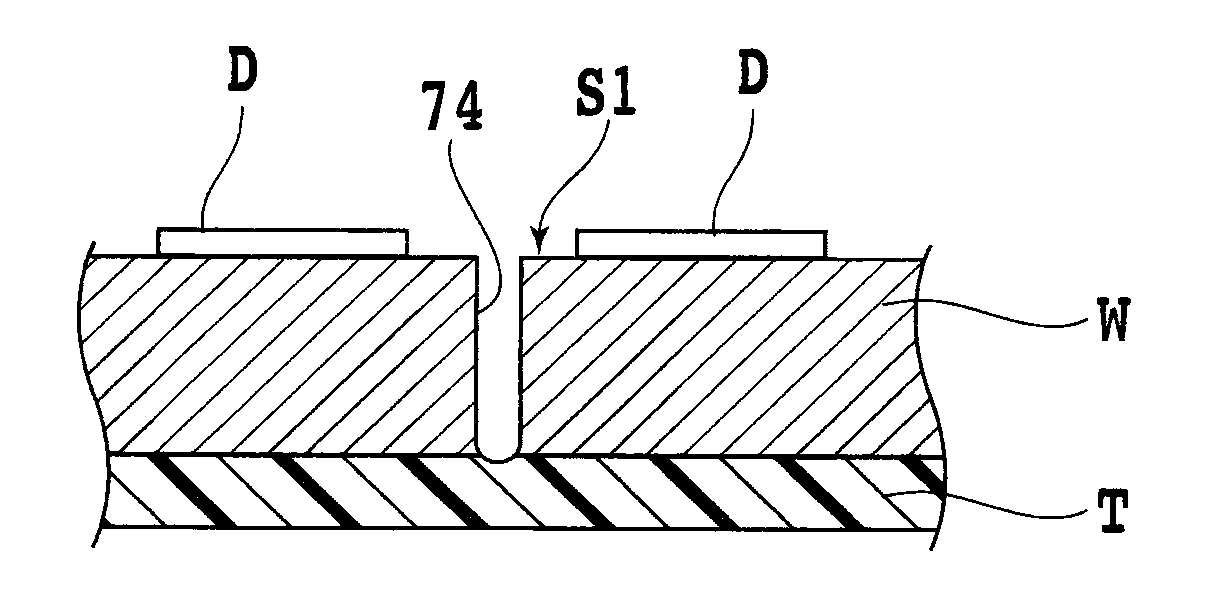
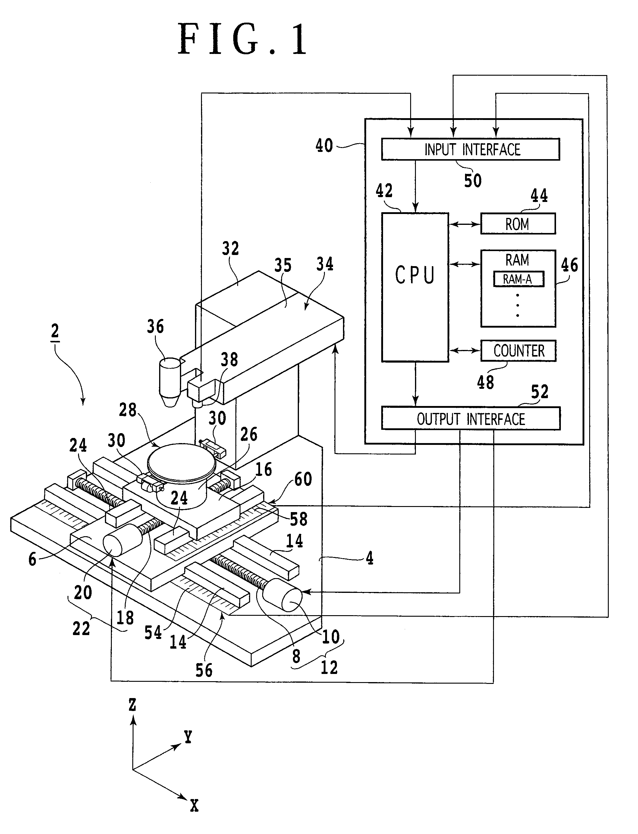
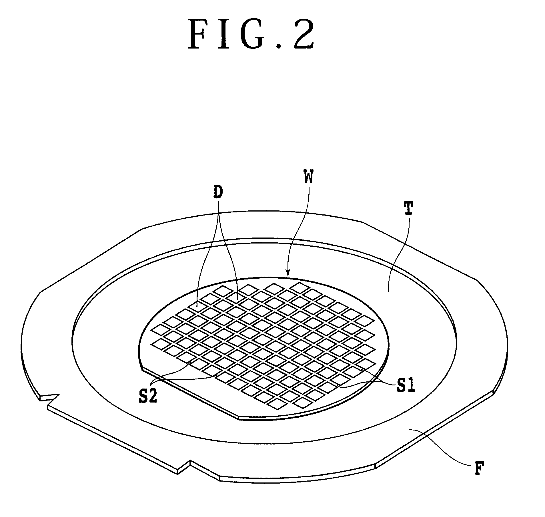
[0025]A preferred embodiment of the present invention will now be described in detail with reference to the drawings. FIG. 1 is a schematic perspective view of a laser processing apparatus 2 for performing the laser processing method according to the present invention. The laser processing apparatus 2 includes a stationary base 4 and a first slide block 6 supported to the stationary base 4 so as to be movable in an X direction in FIG. 1. The first slide block 6 is movable in a feeding direction, i.e., in the X direction along a pair of guide rails 14 by feeding means 12 including a ball screw 8 and a pulse motor 10.

[0026]A second slide block 16 is supported to the first slide block 6 so as to be movable in a Y direction in FIG. 1. The second slide block 16 is movable in an indexing direction, i.e., in the Y direction along a pair of guide rails 24 by indexing means 22 including a ball screw 18 and a pulse motor 20. A chuck table 28 is supported through a cylindrical support member 2...


PUM

PropertyMeasurementUnit
Timeaaaaaaaaaa
Wavelengthaaaaaaaaaa
Energy densityaaaaaaaaaa

Abstract

A laser processing method for a semiconductor wafer including a groove forming step of applying a pulsed laser beam having an absorption wavelength to the semiconductor wafer along a division line formed on the semiconductor wafer to thereby form a laser processed groove along the division line on the semiconductor wafer, wherein the pulse width of the pulsed laser beam to be applied in the groove forming step is set to 2 ns or less, and the peak energy density per pulse of the pulsed laser beam is set less than or equal to an inflection point where the depth of the laser processed groove steeply increases with an increase in the peak energy density.

Description

BACKGROUND OF THE INVENTION[0001]1. Field of the Invention[0002]The present invention relates to a laser processing method for a semiconductor wafer including a groove forming step of applying a laser beam to the semiconductor wafer along a plurality of division lines to thereby form a plurality of laser processed grooves along these division lines on the semiconductor wafer.[0003]2. Description of the Related Art[0004]In a semiconductor device fabrication process, a plurality of crossing division lines called streets are formed on the front side of a substantially disk-shaped semiconductor wafer such as a silicon wafer and a gallium arsenide wafer to partition a plurality of regions where devices such as ICs and LSIs are respectively formed. The semiconductor wafer is divided into the individual devices along the division lines by using a cutting apparatus or a laser processing apparatus, and these devices are widely used in various electrical equipment such as mobile phones and pe...

Claims


Application Information

Patent Timeline
IPC IPC(8): H01L21/26B23K26/00B23K26/364
CPCB23K26/0042B23K26/0635B23K26/4075H01L2221/68336H01L21/67144H01L21/6836H01L21/78H01L21/67132B23K26/0006B23K26/0624B23K26/40B23K2103/50B23K2103/56
Inventor MORIKAZU, HIROSHI
Owner DISCO CORP
Why Eureka
Try Eureka