Wafer dividing method

Inactive Publication Date: 2009-07-23
DISCO CORP
View PDF4 Cites 14 Cited by
  • Summary
  • Abstract
  • Description
  • Claims
  • Application Information

AI Technical Summary

Benefits of technology

[0007]It is therefore an object of the present invention to provide a wafer dividing method using an dicing before grinding technique which can improve the die strength of each device.
[0009]According to the present invention, the chipping generated on both sides of each kerf and the grinding strain generated on the back side of the wafer can be removed, so that the die strength of each device can be improved from conventional 600 MPa to 1000 MPa.

Problems solved by technology

In such a conventional dicing before grinding method, however, chipping is generated on both sides of each kerf formed along each street and a grinding strain due to the grinding step is also generated on the back side of the wafer.
Such chipping and a grinding strain cause a reduction in die strength (strength against breaking) of each device.

Method used


Image

  • Wafer dividing method
  • Wafer dividing method
  • Wafer dividing method

Examples


Embodiment Construction

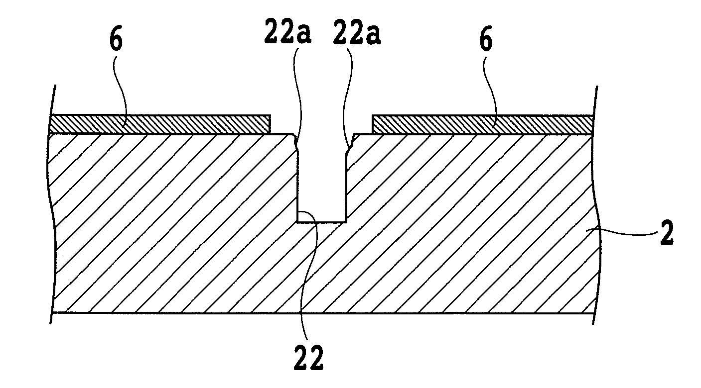
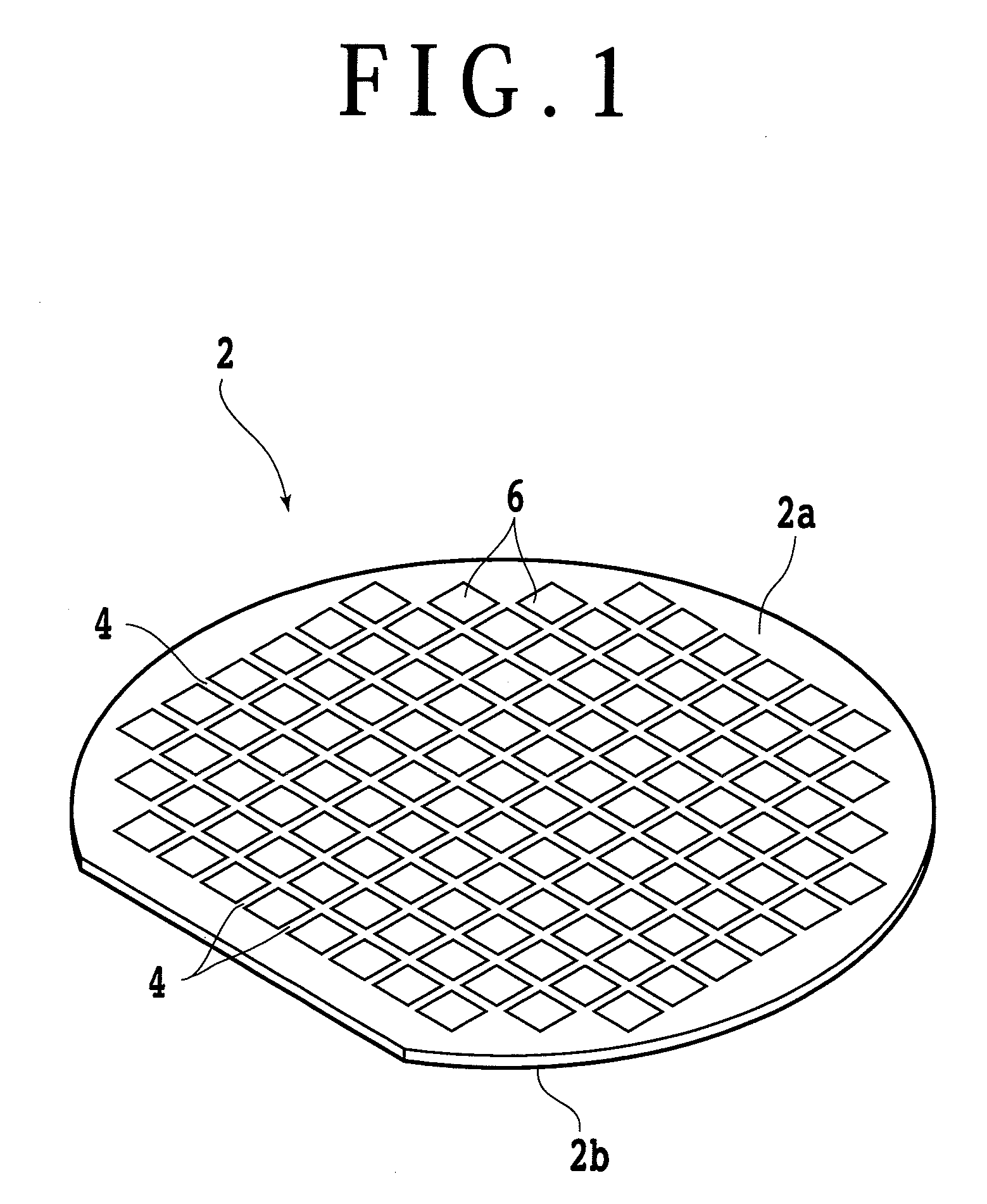
[0025]A preferred embodiment of the wafer dividing method according to the present invention will now be described in detail with reference to the attached drawings. FIG. 1 shows a perspective view of a semiconductor wafer as a wafer. For example, the semiconductor wafer 2 shown in FIG. 1 is a silicon wafer having a thickness of 600 μm. A plurality of crossing streets 4 are formed on the front side 2a of the wafer 2, thereby partitioning a plurality of rectangular areas in which a plurality of devices 6 such as ICs and LSIs are respectively formed.

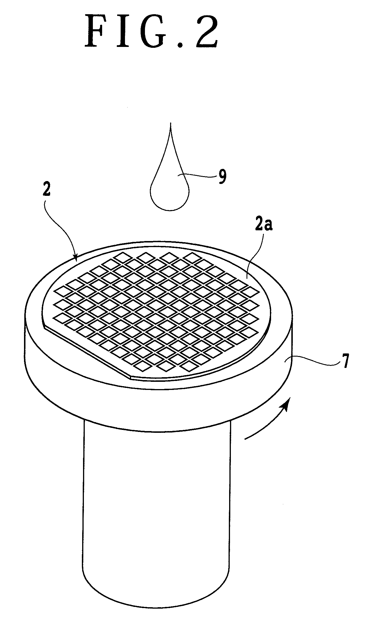
[0026]In the wafer dividing method according to this preferred embodiment, a resist film coating step for coating the front side 2a of the wafer 2 with a resist film as a protective film is performed as a first step. More specifically, as shown in FIG. 2, the wafer 2 is mounted on a spinner table 7 in the condition where the front side 2a of the wafer 2 is oriented upward. The wafer 2 is held on the spinner table 7 by suction vacuum. In th...


PUM


Abstract

A wafer dividing method for dividing a wafer into individual devices, the front side of the wafer being formed with a plurality of crossing streets for partitioning a plurality of areas where the devices are respectively formed. The wafer dividing method includes the steps of coating the front side of the wafer with a protective film, cutting the front side of the wafer with the protective film along the streets to form a plurality of kerfs each having a depth corresponding to the finished thickness of each device, removing chipping from each kerf by plasma etching, attaching a protective tape to the front side of the wafer, grinding the back side of the wafer to expose each kerf to the back side of the wafer, thereby dividing the wafer into the individual devices, and removing a grinding strain from the back side of the wafer.

Description

BACKGROUND OF THE INVENTION[0001]1. Field of the Invention[0002]The present invention relates to a wafer dividing method for dividing a wafer into individual devices, the front side of the wafer being formed with a plurality of crossing streets for partitioning a plurality of areas where the devices are respectively formed.[0003]2. Description of the Related Art[0004]In a semiconductor device fabrication process, a plurality of crossing streets (dividing lines) are formed on the front side of a substantially disk-shaped semiconductor wafer to partition a plurality of areas where devices such as ICs and LSIs are respectively formed, and these areas are separated from each other along the streets to thereby produce the individual devices. As a dividing apparatus for dividing the semiconductor wafer into the individual devices, a cutting apparatus called a dicing apparatus is generally used. The cutting apparatus includes a cutting blade having a very thin cutting edge for cutting the ...

Claims


Application Information

Patent Timeline
IPC IPC(8): H01L21/02
CPCH01L21/78H01L21/67092
Inventor FUJISAWA, SHINICHIONO, TAKASHI
Owner DISCO CORP
Why Eureka
Try Eureka