Method of wafer dicing and die

a technology of die and scribe line, which is applied in the direction of semiconductor/solid-state device testing/measurement, semiconductor device details, semiconductor devices, etc., can solve the problems of large time-consuming and laborious, damage to the die region adjacent to the scribe line, and difficulty in using laser dicing or mechanical dicing to cut a wafer with scribe line of small size, etc., to achieve the effect of reducing the time required to cut the wafer using laser dicing or mechanical

Active Publication Date: 2020-06-16
WINBOND ELECTRONICS CORP
View PDF4 Cites 5 Cited by
  • Summary
  • Abstract
  • Description
  • Claims
  • Application Information

AI Technical Summary

Benefits of technology

[0011]In view of the above, the disclosure removes the complex test structure in the scribe region by performing a plurality of etching cycles of the first etching process and the second etching process, so that the die cut from the wafer has a flat surface. As such, the strength of the die is increased, and the die is able to withstand greater stress, so as to avoid cracking.

Problems solved by technology

If laser dicing or mechanical dicing is used to cut the wafer, since the laser beam and the dicing tool themselves have a certain width, the die region adjacent to the scribe line may be damaged when the width of the scribe line is small.
In other words, it is difficult to use laser dicing or mechanical dicing to cut a wafer having scribe line of small size.
On the other hand, the time required to cut the wafer using laser dicing or mechanical dicing is greatly extended as the path length of the scribe line increases, as such, the cost of wafer dicing is increased.
Furthermore, when the wafer is cut by mechanical dicing, there may be an issue of wafer chipping or cracking due to the mechanical stress generated by the dicing tool, which may cause the damage of the die.
When the wafer is cut by laser dicing, the thermal effect of the laser may be transmitted to the die region to adversely affect the die.
Moreover, after laser dicing and mechanical dicing, the sidewalls of the die usually have rough surfaces.
However, since the scribe line includes a complex structure of multilayers of metal features of test devices and insulating or dielectric features, how to use plasma dicing to remove the complex structure of the test device and the surrounding insulating features in the scribe line is still a problem need to be solved currently.

Method used


Image

  • Method of wafer dicing and die
  • Method of wafer dicing and die
  • Method of wafer dicing and die

Examples


Embodiment Construction

[0017]The invention will be more fully described with reference to the drawings of the embodiments. However, the invention may be embodied in a variety of different forms and should not be limited to the embodiments described herein. The thickness of layers and regions in the drawings may be exaggerated for clarity. The same or similar component numbers indicate the same or similar components. Accordingly, no further description thereof is provided hereinafter.

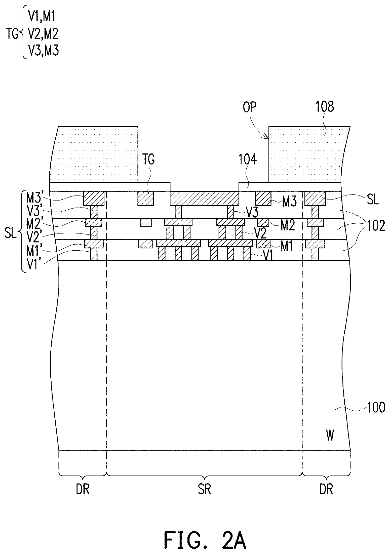
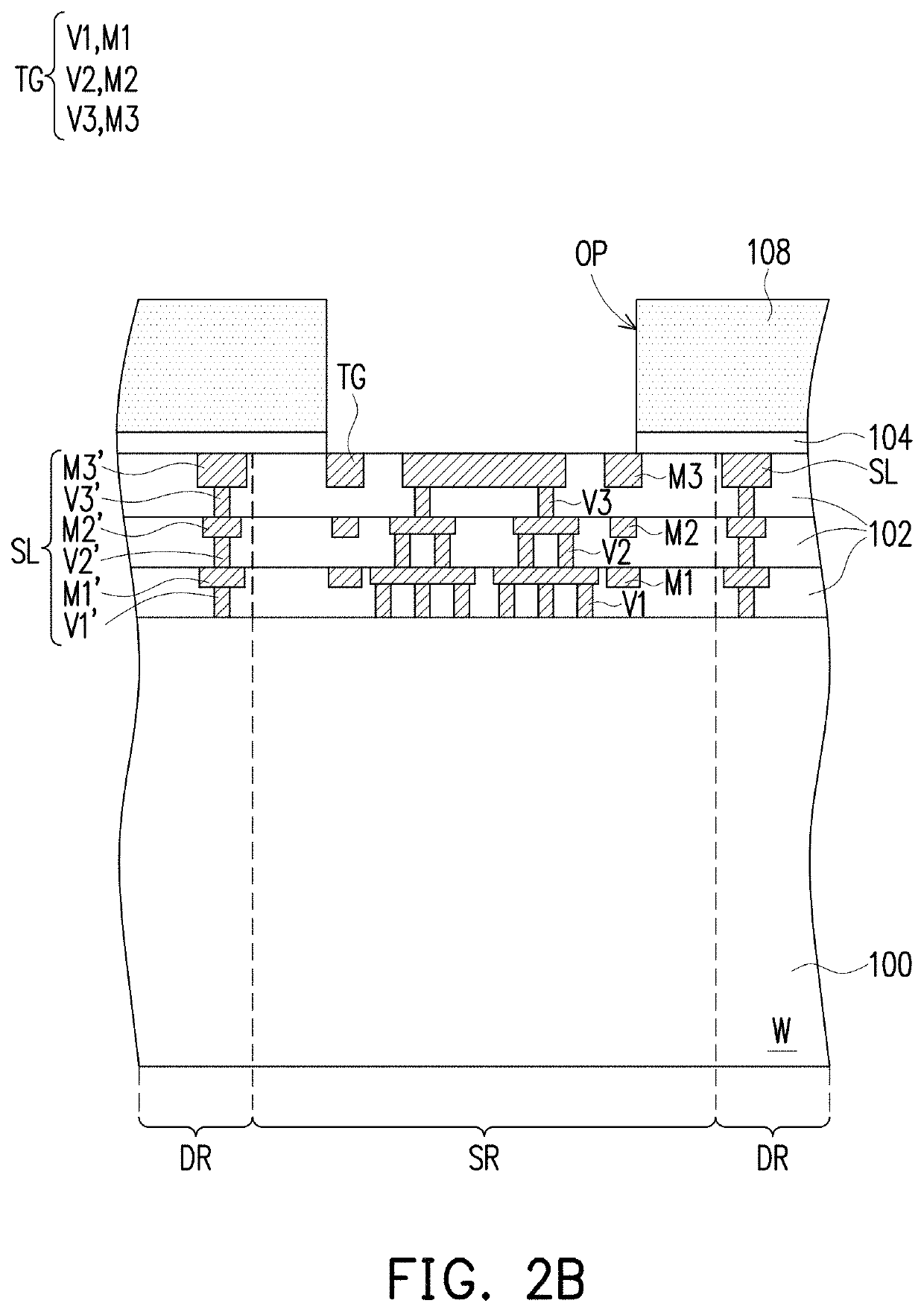
[0018]FIG. 2A to FIG. 2F are schematic cross-sectional views illustrating a method of wafer dicing according to some embodiments of the disclosure. FIG. 3A to FIG. 3F are enlarged schematic views illustrating a method of removing test devices and dielectric layers in a scribe line during wafer dicing according to some embodiments of the disclosure.

[0019]Referring to FIG. 2A, a wafer W is provided. The wafer W includes a substrate 100. The substrate 100 is a semiconductor substrate, such as a doped silicon substrate, an undoped...


PUM

PropertyMeasurementUnit
widthaaaaaaaaaa
widthaaaaaaaaaa
surface roughnessaaaaaaaaaa

Abstract

A method of wafer dicing and a die are provided. The method includes the following processes. A wafer is provided, the wafer includes a plurality of die regions and a scribe region between the die regions. The scribe region includes a substrate, and a dielectric layer and a test structure on the substrate, the test structure is disposed in the dielectric layer. A first removal process is performed to remove the test structure and the dielectric layer around the test structure, so as to expose the substrate. The first removal process includes performing a plurality of etching cycles, and each etching cycle includes performing a first etching process to remove a portion of the test structure and performing a second etching process to remove a portion of the dielectric layer. A second removal process is performed to remove the substrate in the scribe region, so as to form a plurality of dies separated from each other.

Description

BACKGROUNDTechnical Field[0001]The embodiments of the disclosure relates to a method of wafer dicing and a die.Description of Related Art[0002]After the fabrication of a wafer is completed, dicing technique is used to cut the wafer into a plurality of individual dies along the scribe line. Current wafer dicing techniques include, for example, mechanical dicing such as dicing using a blade, laser dicing, plasma dicing or the like.[0003]With the miniaturization of the critical dimension of the semiconductor device, more dies can be formed on a single wafer, thereby making the width of the scribe line smaller and smaller, and the path length of the scribe line is also increased. If laser dicing or mechanical dicing is used to cut the wafer, since the laser beam and the dicing tool themselves have a certain width, the die region adjacent to the scribe line may be damaged when the width of the scribe line is small. In other words, it is difficult to use laser dicing or mechanical dicing ...

Claims


Application Information

Patent Timeline
Patent Type & Authority Patents(United States)
IPC IPC(8): H01L21/78H01L23/00H01L23/544H01L21/3065H01L21/66H01L21/311H01L21/3213
CPCH01L23/544H01L21/78H01L21/3065H01L22/32H01L23/562H01L21/32136H01L21/31116H01L2223/5446H01L22/34H01L23/585H01L21/561
Inventor WEI, CHENG-HONGCHEN, HUNG-SHENGCHEN, CHING-WEICHANG, SHUO-CHE
Owner WINBOND ELECTRONICS CORP
Why Eureka
Try Eureka