
Mass memory device and storage system

Inactive Publication Date: 2010-11-25
SAFRAN ELECTRONICS & DEFENSE
View PDF3 Cites 0 Cited by
  • Summary
  • Abstract
  • Description
  • Claims
  • Application Information

AI Technical Summary

Benefits of technology

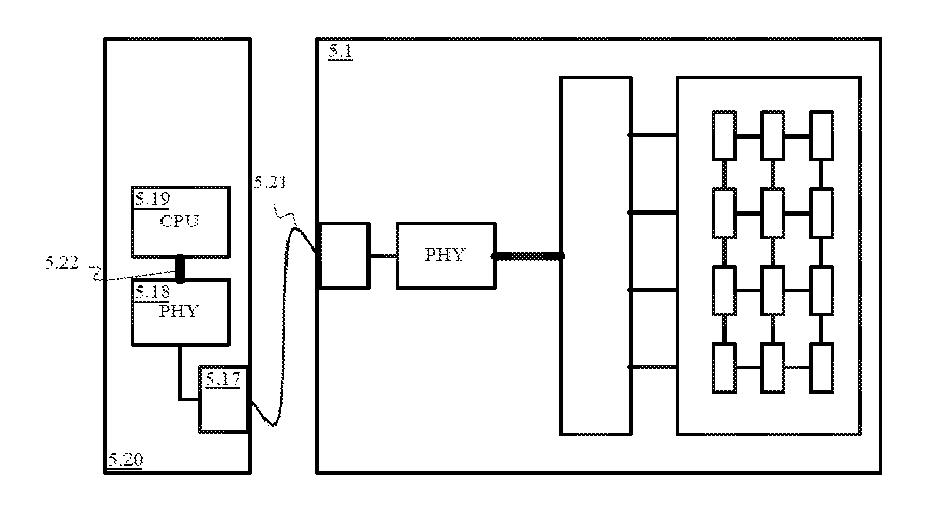
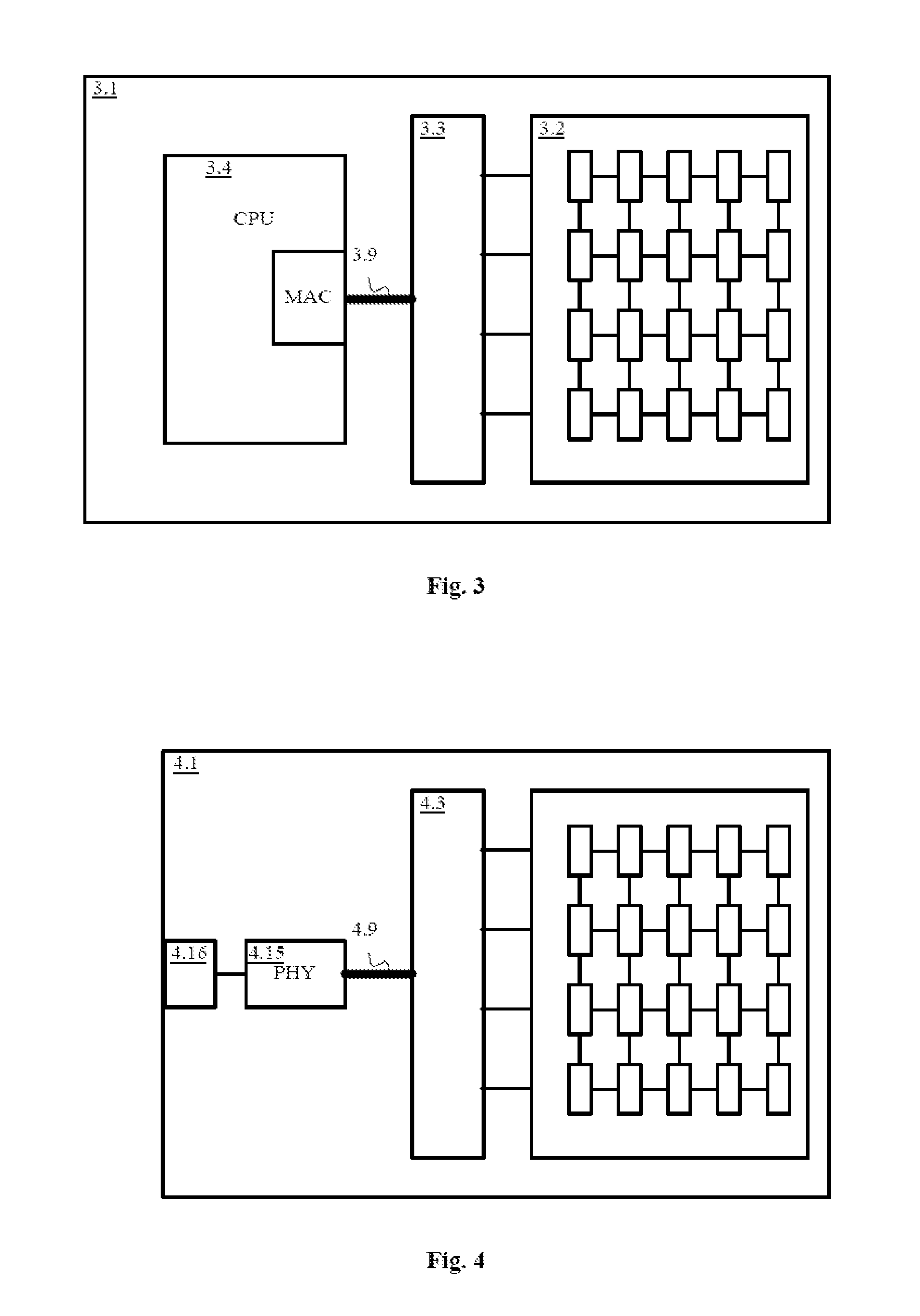
[0006]The present disclosure sets out to propose a mass memory device that can easily be offset while remaining of simple design. This device has a bus from the family of MII (Media Independent Interface) buses connected to the programmable component managing the reading and writing on the memory. This architecture makes it possible to implement the control module of the device at a distance, the communication between the controller and the programmable component being able to be offset on an Ethernet link directly connected to the MII-family bus. This architecture may be adapted for the design of mass memory devices comprising the control module, also devices where the control module is offset and again mass memory devices of the NAS type with simplified architecture. The simple architecture of these devices offer improved security, the certification of which is easier.
[0013]In one embodiment, the host control module on the one hand and the physical management module for the memory on the other hand also have means of managing the command protocol in UDP data packets encapsulated in IP data packets transported in Ethernet packets. This management of the IP protocol makes it possible to pass commands of the protocol over an IP network between the host system and the mass memory device.
[0014]In one embodiment, the host system also comprises at least a second Ethernet socket for connecting the host system to a communication network and means of managing a complete network protocol stack by the control module of the host system, making it possible to expose the mass memory device on the communication network, thus forming a mass memory device accessible by network.BRIEF DESCRIPTION OF THE DRAWINGS

Problems solved by technology

This offsetting is not possible using the IDE link limited to a distance of 50 cm.
These mass memory devices allow external connection to an information system; however, the maximum offsetting distance remains limited to a distance of around five metres.

Method used


Image

  • Mass memory device and storage system
  • Mass memory device and storage system
  • Mass memory device and storage system

Examples


Embodiment Construction

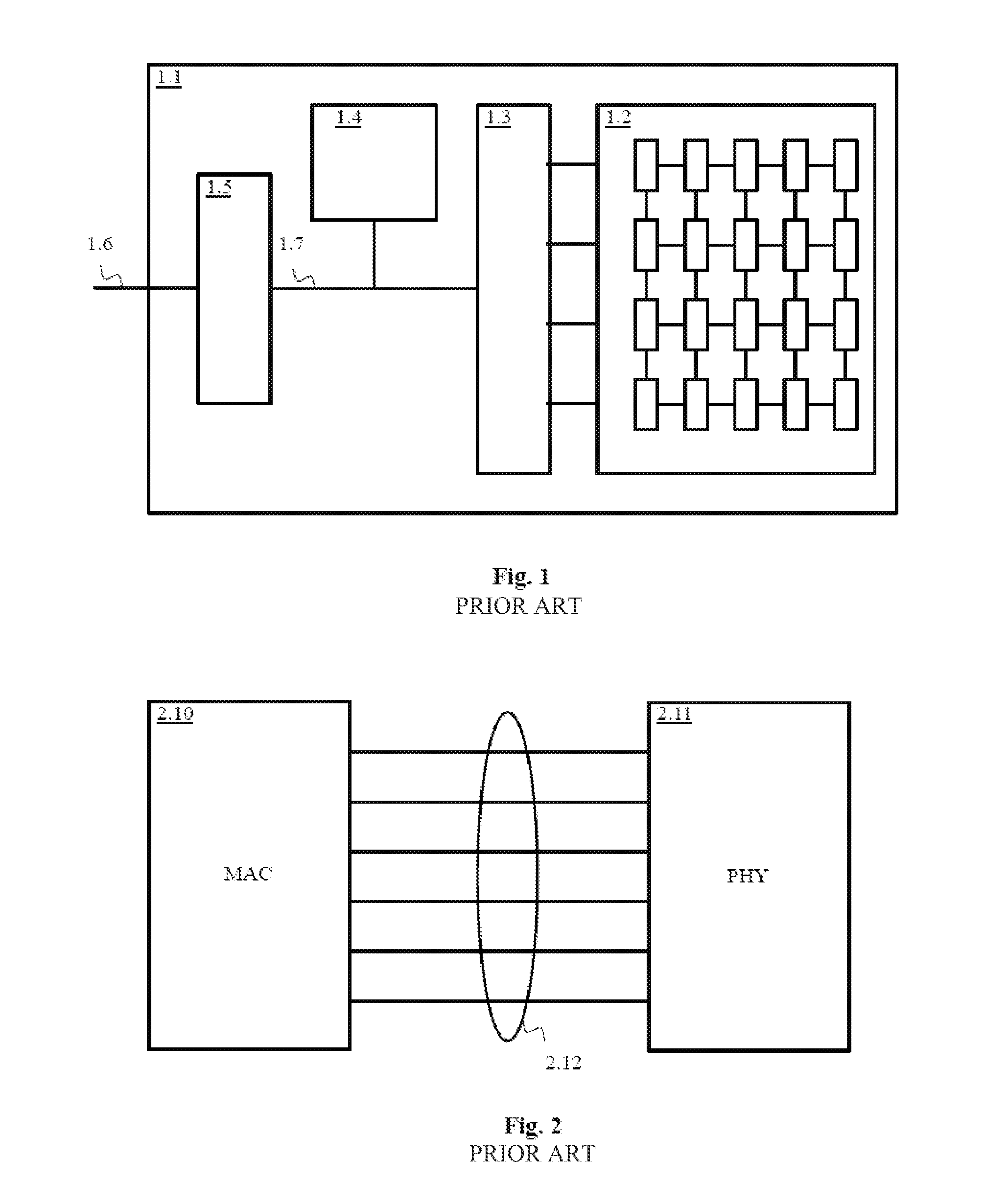
[0024]The MII (Media Independent Interface) bus is standardised by the IEEE (Institute of Electrical and Electronics Engineers) under the reference IEEE 802.3u. This bus is used for implementing links according to the Ethernet standard defined by the IEEE under the reference 802.3. This bus was developed to manage communication between a physical Ethernet module and an MAC (Media Access Control) Ethernet module. This architecture is illustrated by FIG. 2. In this figure, an MAC Ethernet management module 2.10 is connected to a physical management module 2.11 by an MII bus 2.12. This bus enables 4-bit words to be exchanged in both directions timed by a 25 MHz clock. The physical management module 2.11 manages the sending and reception of the signals transporting the Ethernet data packets over the physical medium. The MAC management module 2.10 takes care of the management of these packets, and composing them. It is controlled by top layers of the stack of network protocols used, typi...


PUM


Abstract

A mass memory device is disclosed as including a memory module, a management module for physical management of the memory module, and a control module for controlling the management module. The management module is connected for communication with the control module by an MII-family bus.

Description

CROSS-REFERENCE TO RELATED APPLICATION[0001]This application is a National Stage filing of International Application Serial No. PCT / EP2009 / 051156, filed Feb. 2, 2009, designating the United States, and which claims priority to French patent application Ser. No. 08 / 00593, filed Feb. 5, 2008 by the same inventor hereto, the disclosures of which are expressly incorporated herein by reference.FIELD OF THE DISCLOSURE[0002]The present disclosure concerns computer mass memory devices and more particularly the architecture thereof.BACKGROUND AND SUMMARY[0003]The internal architecture of a mass memory device, such as a disk on a SSD (Solid State Drive) memory component, is illustrated in FIG. 1. This architecture is derived from the architecture of hard disks, the main features of which it reproduces. The disk on memory component 1.1 is composed of a physical mass memory module 1.2, in this case a bank of memory components containing the memory components proper. The memory components are ge...

Claims


Application Information

Patent Timeline
IPC IPC(8): G06F12/00G06F12/02G06F15/167
CPCG06F13/385
Inventor COURTEILLE, JEAN-MARIEGUILLOT, FRANCOIS
Owner SAFRAN ELECTRONICS & DEFENSE
Learn More