Controlling Warpage in BGA Components in a Re-flow Process

a re-flow and component technology, applied in sustainable manufacturing/processing, final product manufacturing, semiconductor/solid-state device details, etc., can solve the problems of insufficient solder and drawbacks of conventional surface mounting technology, and achieve the effect of improving the yield of surface mounting processes

Active Publication Date: 2010-12-02
TAIWAN SEMICON MFG CO LTD +1
View PDF11 Cites 11 Cited by
  • Summary
  • Abstract
  • Description
  • Claims
  • Application Information

AI Technical Summary

Benefits of technology

[0011]The advantageous features of the present invention include improved yield in the surface mounting processes for mounting

Problems solved by technology

The conventional surface mounting technology suffers from drawbacks.
This is often characteri

Method used


Image

  • Controlling Warpage in BGA Components in a Re-flow Process
  • Controlling Warpage in BGA Components in a Re-flow Process
  • Controlling Warpage in BGA Components in a Re-flow Process

Examples


Embodiment Construction

[0019]The making and using of the embodiments of the present invention are discussed in detail below. It should be appreciated, however, that the embodiments provide many applicable inventive concepts that can be embodied in a wide variety of specific contexts. The specific embodiments discussed are merely illustrative of specific ways to make and use the invention, and do not limit the scope of the invention.

[0020]A novel surface mounting method is provided in accordance with an embodiment. The variations of the embodiment are then discussed. Throughout the various views and illustrative embodiments of the present invention, like reference numbers are used to designate like elements.

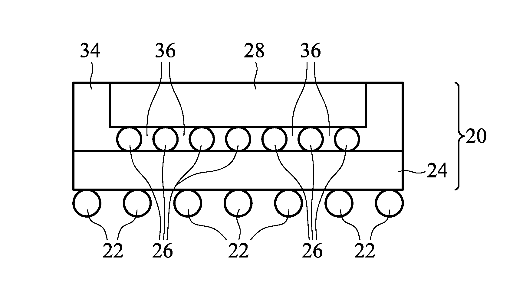
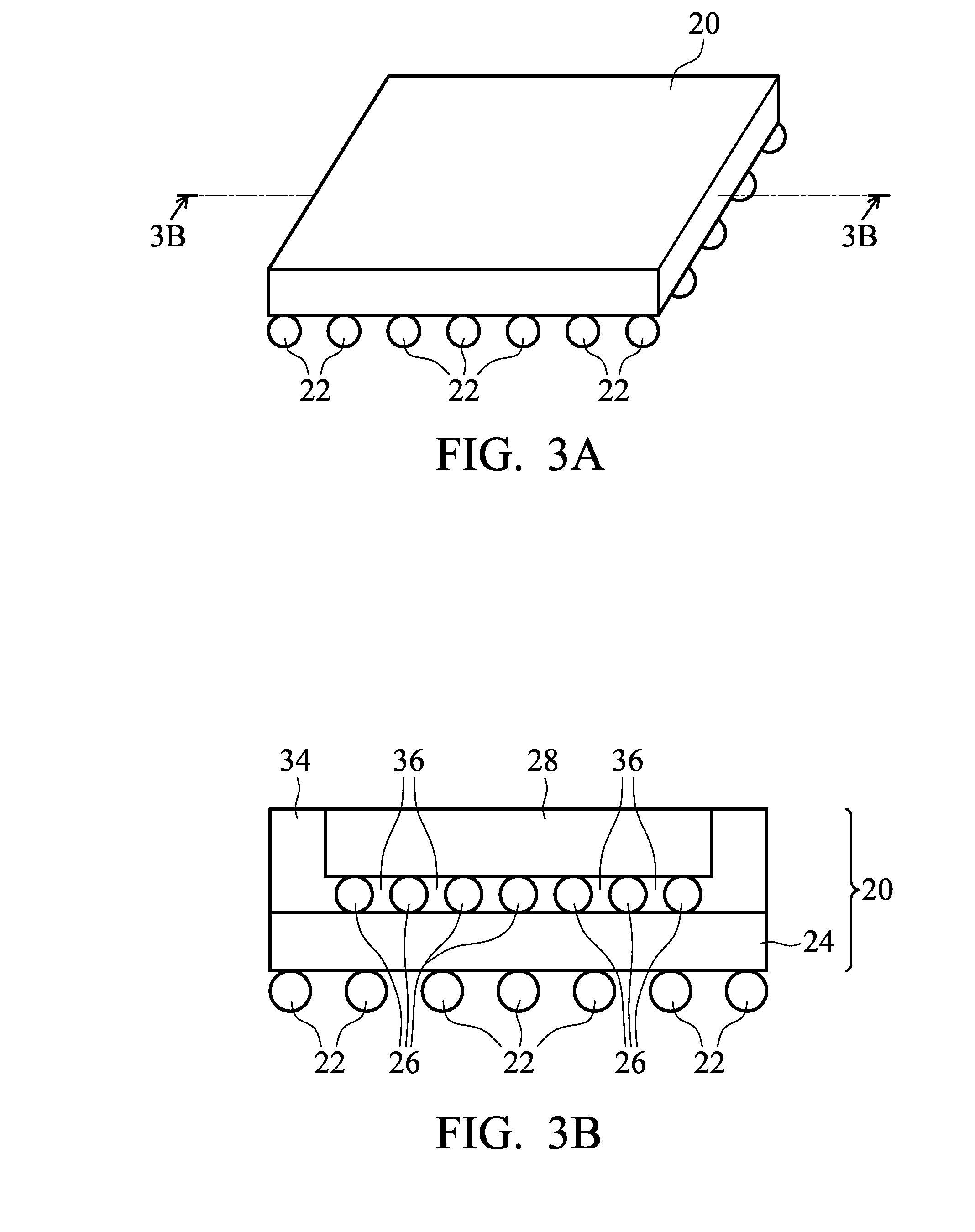
[0021]FIG. 3A illustrates a perspective view of ball grid array (BGA) module 20. FIG. 3B illustrates a cross-sectional view of an exemplary BGA module 20, which includes package substrate 24 and die 28 mounted on package substrate 24. BGA balls 22 are mounted on one side of BGA module 20, and are electr...


PUM

PropertyMeasurementUnit
Temperatureaaaaaaaaaa
Adhesivityaaaaaaaaaa

Abstract

A method of manufacturing an integrated circuit package includes providing a ball grid array (BGA) module including BGA balls on a side of the BGA module; providing a base substrate; and placing the BGA module on the base substrate. The BGA balls are placed between the BGA module and the base substrate. An adhesive is applied between and contacting the BGA module and the base substrate. The adhesive is then cured. The BGA balls are re-flowed after the step of curing the adhesive.

Description

[0001]This application claims the benefit of U.S. Provisional Application No. 61 / 182,939 filed on Jun. 1, 2009, entitled “Controlling Warpage in BGA Components in a Re-flow Process,” which application is hereby incorporated herein by reference.TECHNICAL FIELD[0002]This invention relates generally to manufacturing processes of integrated circuits, and more particularly to packaging processes, and even more particularly to methods for improving the reliability in mounting ball grid array (BGA) modules onto printed circuit boards (PCBs).BACKGROUND[0003]Modern integrated circuits are formed on semiconductor chips. To increase manufacturing throughput and to lower manufacturing costs, the integrated circuits are manufactured in semiconductor wafers, each containing many identical semiconductor chips. After the integrated circuits are manufactured, semiconductor chips are sawed from the wafers and packaged before they can be used.[0004]In typical packaging processes, semiconductor chips (...

Claims


Application Information

Patent Timeline
IPC IPC(8): H05K7/00H01R43/00
CPCH01L21/563H01L2924/00014H01L2224/13099H01L2924/01322H01L2924/14H01L2924/15311H01L2924/18161H01L2924/3511H05K3/305H05K3/3436H05K3/3494H05K2201/10734H01L23/49816H01L2924/00011H01L2924/01087H01L2224/16225Y02P70/613Y10T29/49165Y10T29/49155Y10T29/49117Y10T29/49144H01L2224/0401Y02P70/50
Inventor KAO, CHIA-JENTSAI, CHEN-FACHEN, CHIEN-WEN
Owner TAIWAN SEMICON MFG CO LTD
Why Eureka
Try Eureka