
Touch sensor panel having a split-electrode structure and a touch sensor device provided with the same
a touch sensor and split-electrode technology, applied in the field of touch sensor panels, can solve the problems of reducing the transparency of the panel, increasing the cost of a process, and reducing so as to improve the linearity of the touch input and enhance the detection accuracy
- Summary
- Abstract
- Description
- Claims
- Application Information
AI Technical Summary
Benefits of technology
Problems solved by technology
Method used
Image

Examples
Embodiment Construction
[0019]Hereinafter, embodiments of the present invention will be described in detail with reference to the accompanying drawings which form a part hereof. The same or corresponding components will be denoted using the same reference numerals and duplicate description will be omitted.
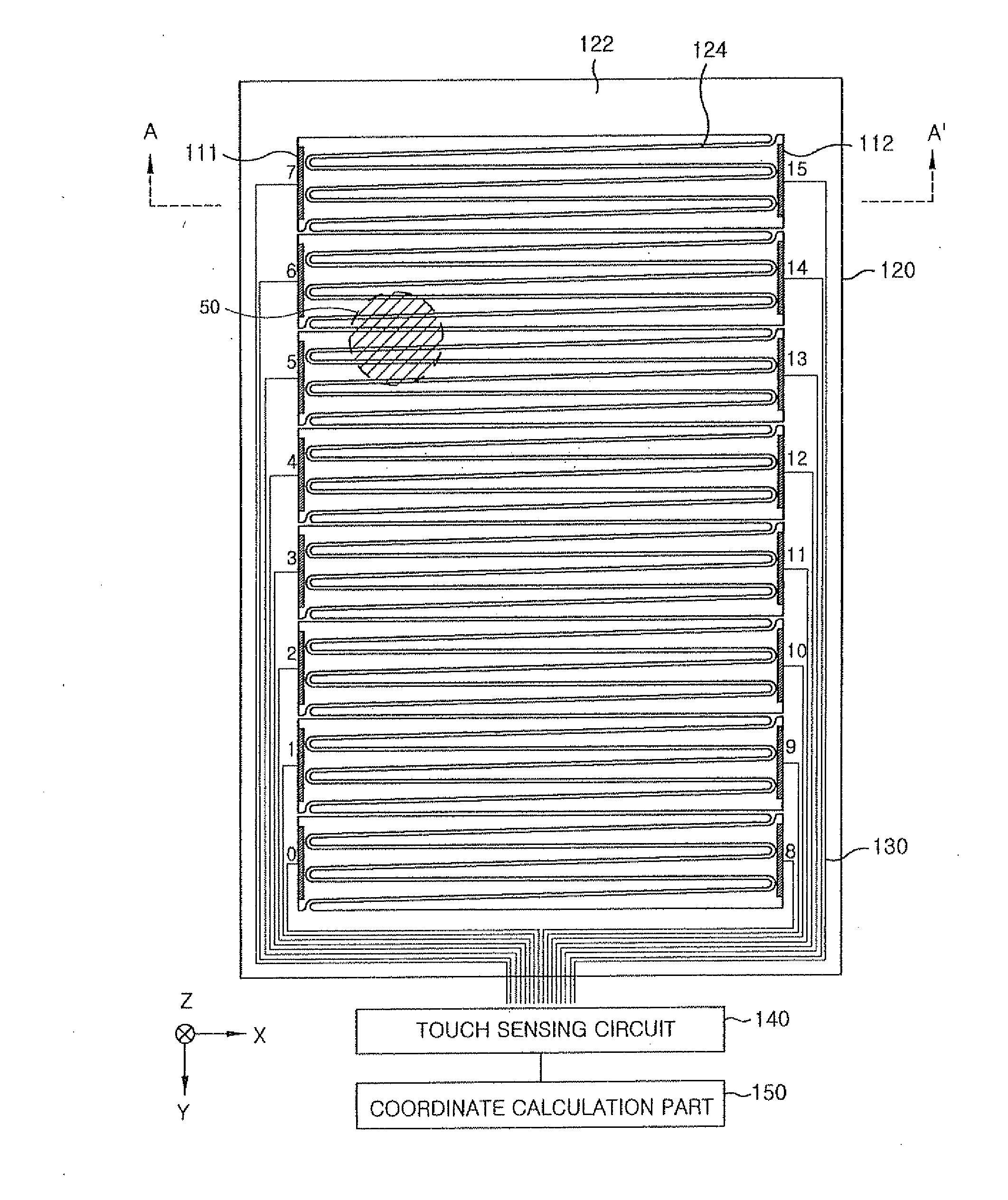
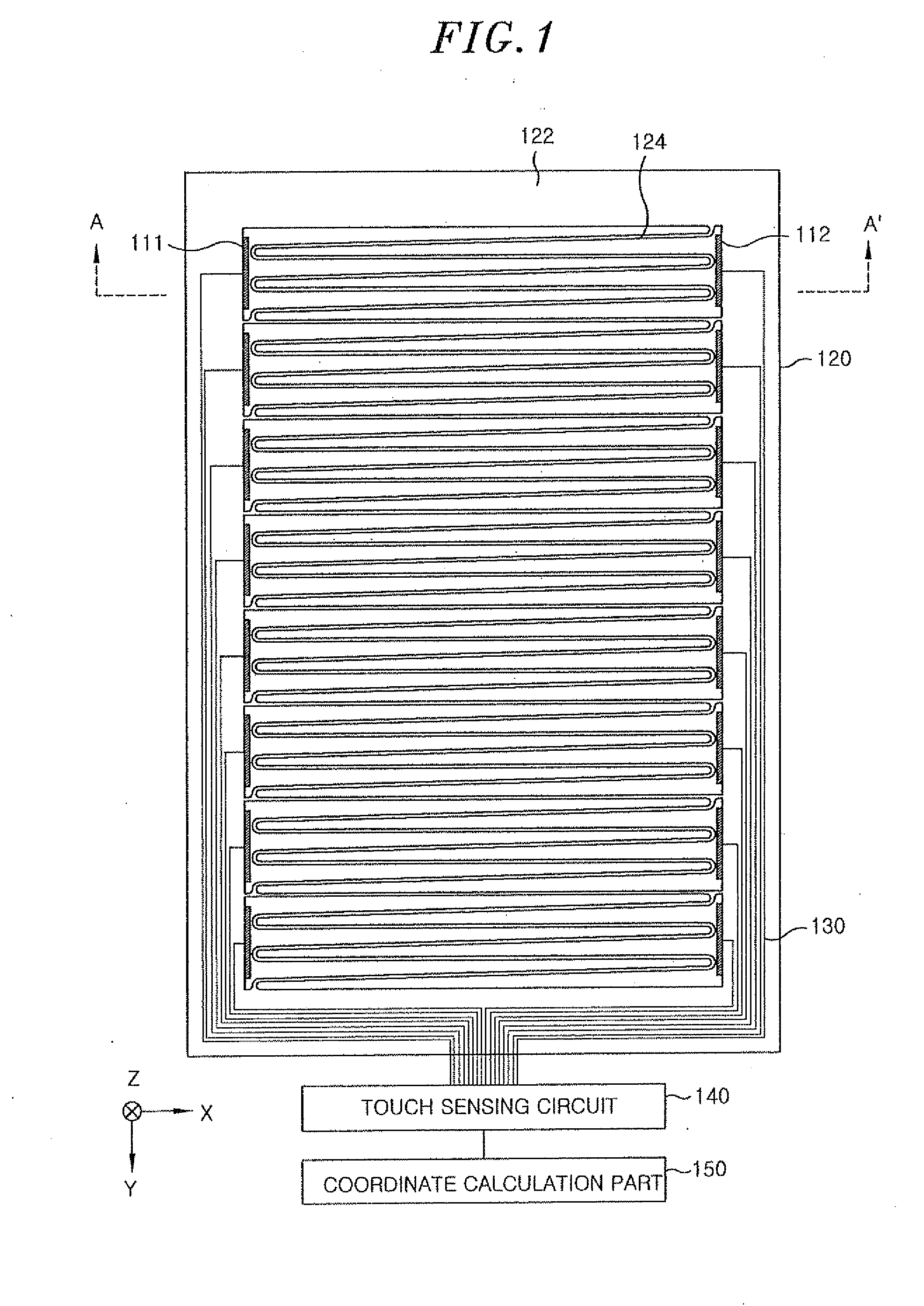
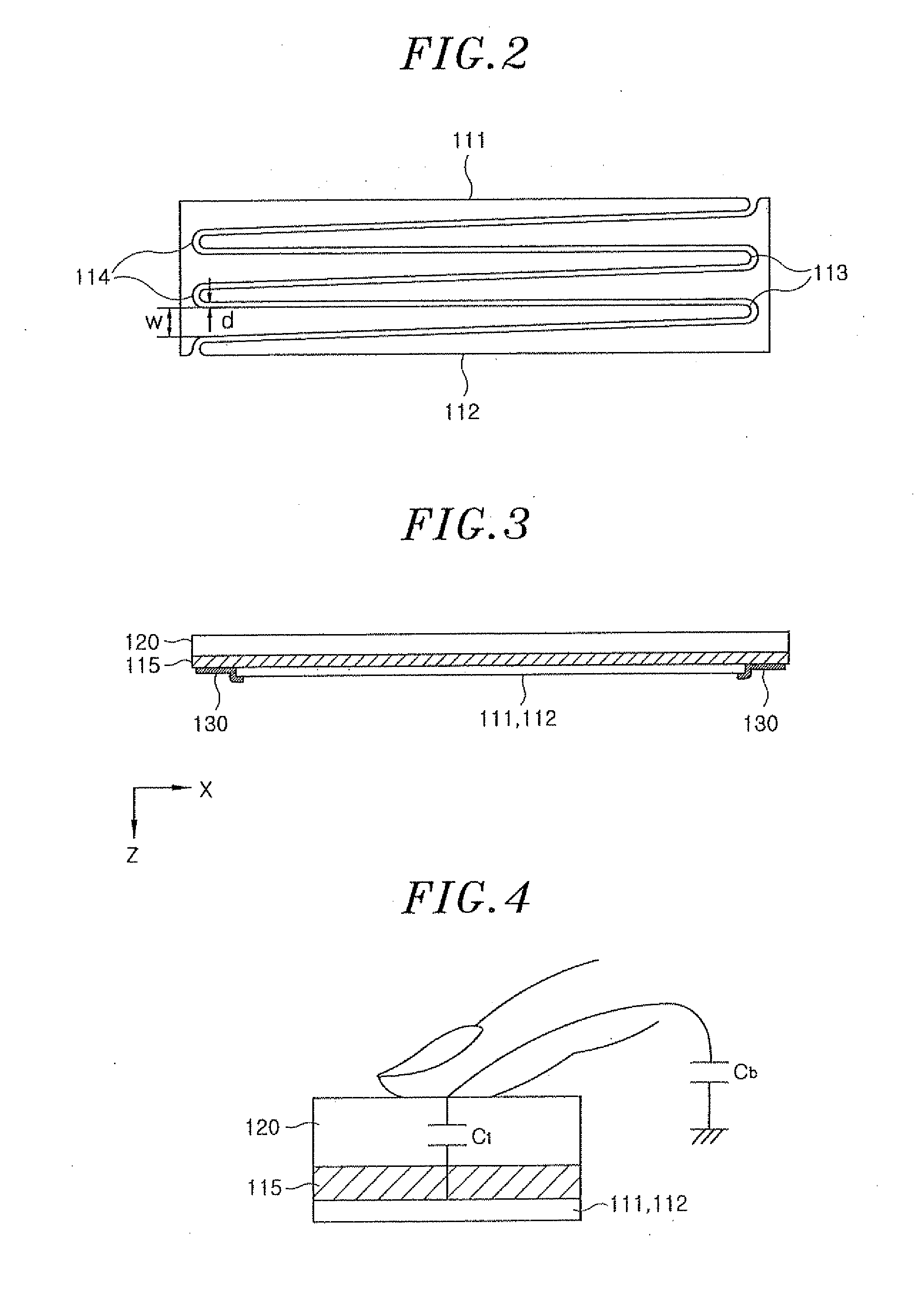
[0020]FIG. 1 shows a schematic plane view of an arrangement of a touch sensing panel in accordance with an embodiment of the present invention; and FIG. 2 is a view for describing in detail the shape and arrangement of the sensing electrodes 111 and 112 shown in FIG. 1. Further, FIG. 3 shows a cross sectional view taken along the A-A′ line shown in FIG. 1. As shown in the drawings, it will be described hereinafter the lateral direction as an X-direction, the vertical direction as a Y-direction, and the thickness direction as a Z-direction.
[0021]Referring to FIG. 1, the respective sensing electrodes 111 and 112 are connected to a conductive wire 130 at each side of the touch sensing panel. The sensing elec...
PUM
 Abstract
Description
Claims
Application Information