Method of driving a liquid crystal panel

Active Publication Date: 2010-12-09
TRIVALE TECH
View PDF10 Cites 12 Cited by
  • Summary
  • Abstract
  • Description
  • Claims
  • Application Information

AI Technical Summary

Benefits of technology

[0009]Accordingly, a display malfunction due to the signal waveform becoming blunt at high temperature is remedied, and display unevenness due to a

Problems solved by technology

Thus, in a case where a liquid crystal display device is used in a wide temperature range from low temperature to high temperature, interconnection resistance becomes high at high temperature to increase an RC time constant, which increases a signal delay as well.
As a result, signal waveforms of the horizontal scanning interconnections become blunt, which causes a failure in writing timing.
Although it is possible to take measures against this by adjusting timings in consideration of a signal delay du

Method used


Image

  • Method of driving a liquid crystal panel
  • Method of driving a liquid crystal panel
  • Method of driving a liquid crystal panel

Examples


first preferred embodiment

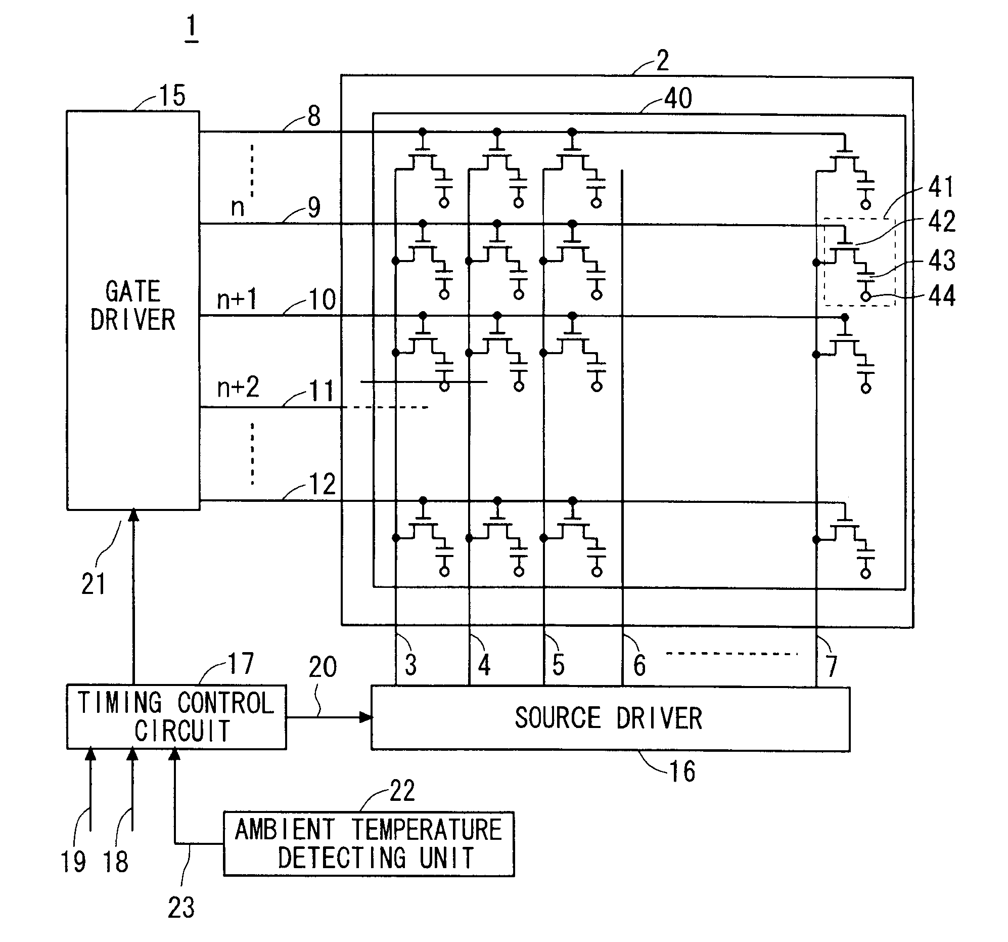
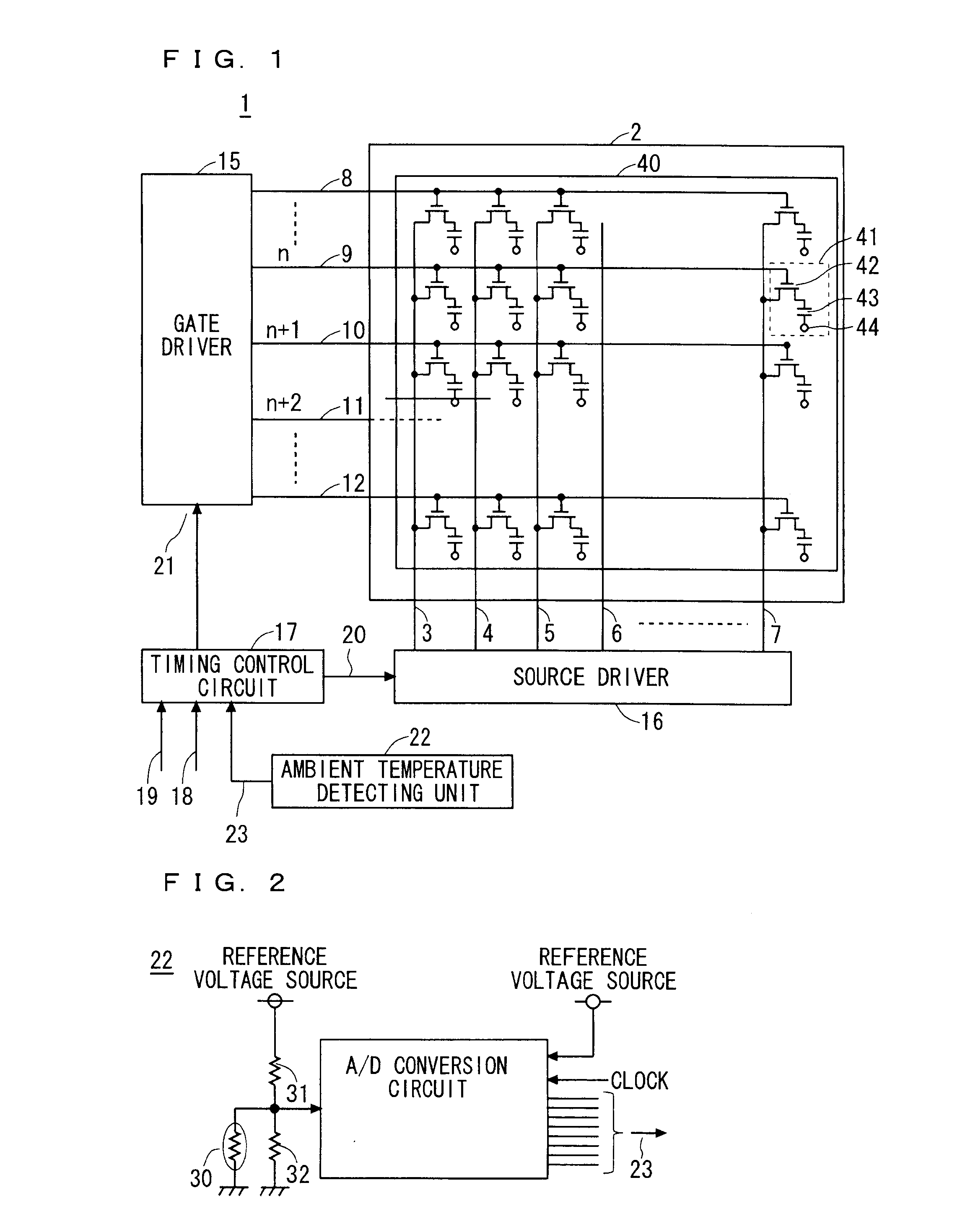
[0016]FIG. 1 is a system configuration diagram showing a schematic configuration of a liquid crystal display device 1 according to a first preferred embodiment. In FIG. 1, a liquid crystal panel 2 is formed by bonding an active matrix substrate 40 and a counter substrate (not shown) opposed thereto with a gap therebetween, and liquid crystal (not shown) is held in the gap. The active matrix substrate 40 includes a plurality of data interconnections 3, 4, 5, 6 and 7 and a plurality of horizontal scanning interconnections 8, 9, 10, 11 and 12 which are formed in matrix to intersect each other. For simplification of description, a configuration of one specific pixel unit is now described in detail, and the entire liquid crystal panel 2 will be described thereafter.

[0017]Here, as to pixels constituting a display area of the liquid crystal panel 2, description is given by means of a representative pixel unit 41 indicated by a broken line. In FIG. 1, the pixel unit 41 is positioned in the ...

second preferred embodiment

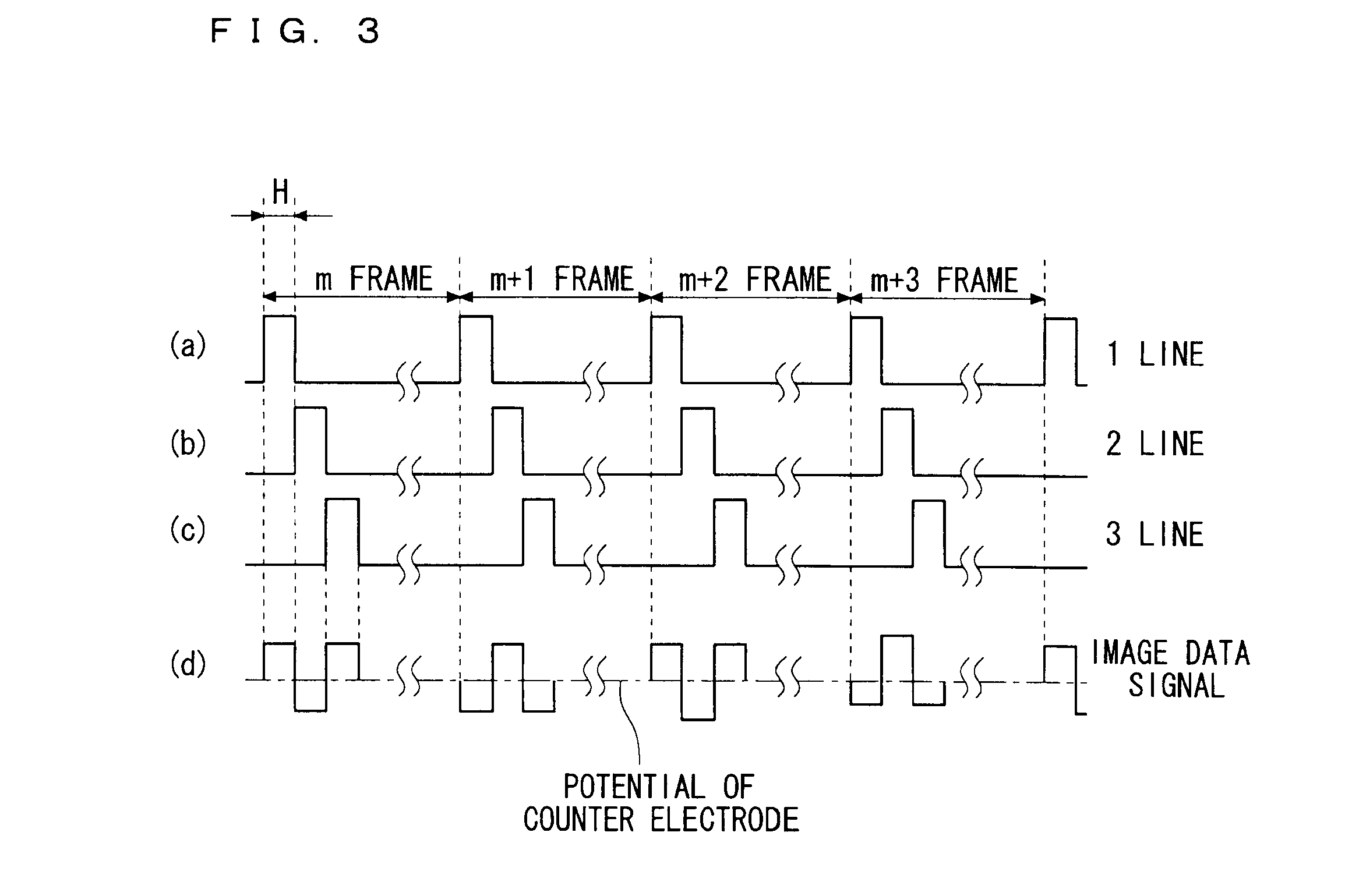
[0037]FIG. 5 is a waveform chart showing time relations between an ambient temperature of the liquid crystal panel and a gate selection signal waveform, an image data signal and a pixel potential of a liquid crystal display device according to a second preferred embodiment. Differently from the gate selection signal waveform of FIG. 3 which has been described in the first preferred embodiment, in the second preferred embodiment, a blanking period which will be described below is provided between gate selection signals between adjacent ones of the horizontal scanning interconnections 9 (n line),10 (n+1 line) and 11 (n+2 line). Other configuration is similar to that of the first preferred embodiment described above, and thus detailed description thereof will be omitted here.

[0038]In FIG. 5, two linear chain lines represent one horizontal cycle period and coincide with a polarity change timing at which an ideal image data signal changes from Vs(+) to Vs(−) or from Vs(−) to Vs(+) as sho...


PUM


Abstract

Provided is a method of driving a liquid crystal panel by providing a gate delay compensation period to a timing at which gate selection signal waveforms supplied to horizontal scanning interconnections change so that a switching element changes from a conduction state to a non-conduction state with respect to a timing at which image data signal waveforms supplied to data interconnections change so that image data corresponding to display contents of a pixel electrode connected to the horizontal scanning interconnections changes to next image data, wherein an ambivalent temperature is detected to make the gate delay compensation period variable in accordance with the ambivalent temperature.

Description

BACKGROUND OF THE INVENTION[0001]1. Field of the Invention[0002]The present invention relates to a method of driving a liquid crystal panel, which is preferably used in driving of an active matrix liquid crystal panel for achieving excellent display quality at ambient temperature in a range of low temperature to high temperature.[0003]2. Description of the Background Art[0004]In writing to pixels of a typical liquid crystal display device using an active matrix liquid crystal panel, a waveform becomes blunt due to interconnection resistance in a gate selection signal as well as an image data signal. For this reason, as commonly known in Japanese Patent Application Laid-Open No. 59-123884, signal timings thereof are set by being shifted somewhat form each other. Specifically, driving is performed such that a gate selection signal goes high to input an image data signal and then the gate selection signal goes low to end the image data signal. However, an influence of a waveform becomi...

Claims


Application Information

Patent Timeline
IPC IPC(8): G09G5/00G09G3/36
CPCG09G2320/041G09G3/3648
Inventor OHTSUKI, HIDEYO
Owner TRIVALE TECH
Why Eureka
Try Eureka