Wafer-level lens module and image pickup module including the same

a technology image pickup module, which is applied in the field of wafer-level lens module that uses polymer lenses to 5 mega pixels, and can solve the problems of high chromatic aberration, polymer lens is easily distorted with respect to shape and show high chromatic aberration, and the difficulty in supporting such a high-resolution camera phone using a wafer-level lens module constructed using only polymer lenses

Inactive Publication Date: 2010-12-09
SAMSUNG ELECTRONICS CO LTD
View PDF27 Cites 108 Cited by
  • Summary
  • Abstract
  • Description
  • Claims
  • Application Information

AI Technical Summary

Benefits of technology

[0010]Aspects of exemplary embodiments may provide a wafer-level lens module which is small and light-weight, suitable for installation in small electronic

Problems solved by technology

However, there are difficulties in applying such a wafer-level lens module that uses polymer lenses to 5 Mega pixels or higher resolution cameras.
The reason is that polymer lenses are easily distorted with respect to shape and show high chromatic

Method used


Image

  • Wafer-level lens module and image pickup module including the same
  • Wafer-level lens module and image pickup module including the same
  • Wafer-level lens module and image pickup module including the same

Examples


numerical example 1

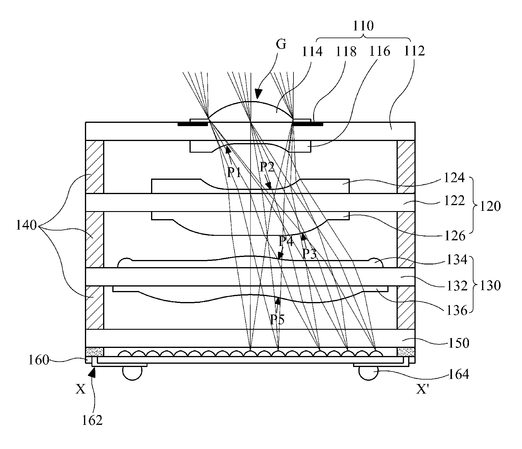
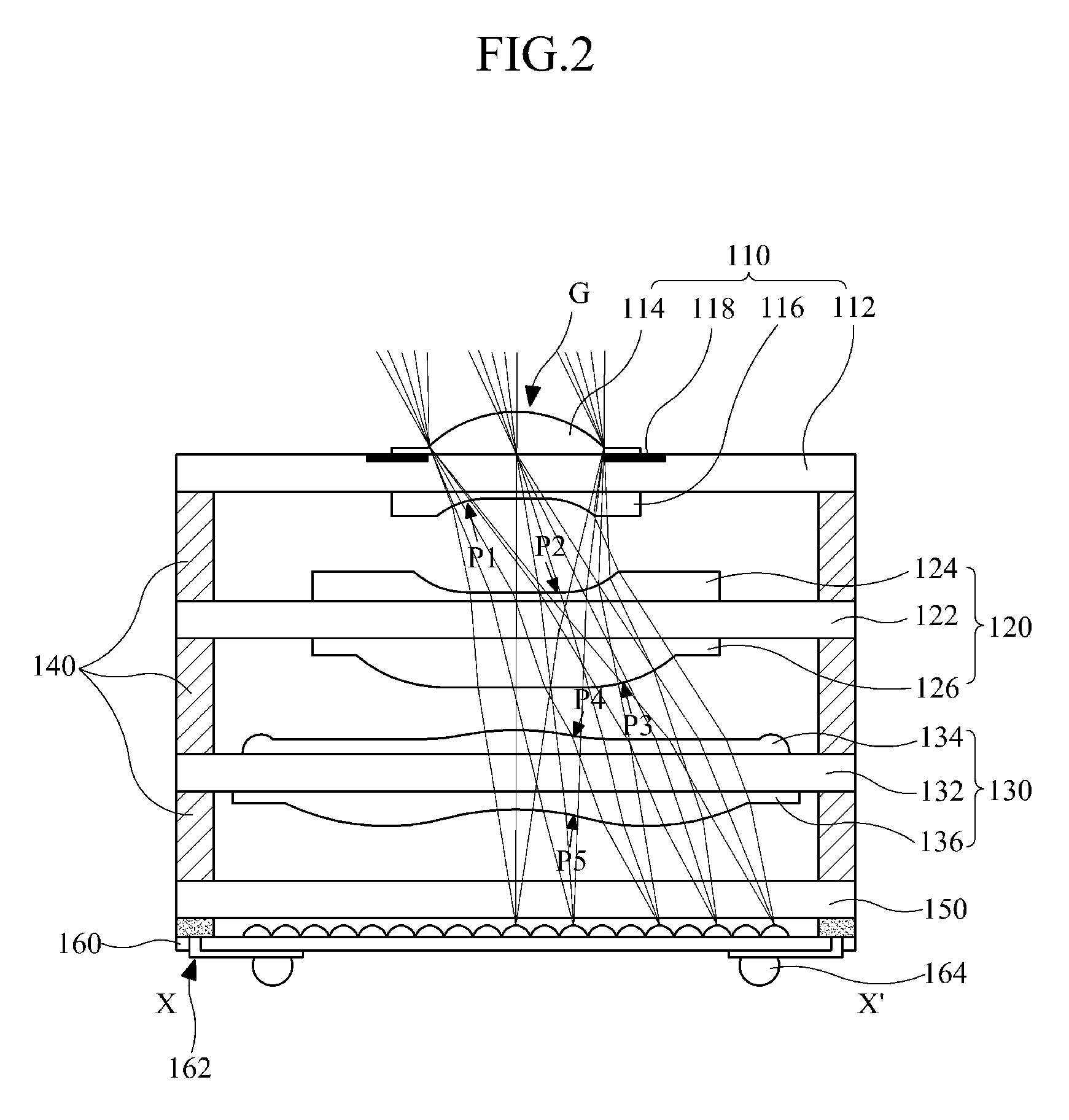
[0050]Table 2 shows geometry parameters that digitize the surface geometries of individual lens elements constructing the exemplary wafer-level lens module illustrated in FIG. 2. This numerical example 1 relates to a wafer-level lens module whose height (a distance from the object-side surface of the first lens group to the image sensor) is 5.15 mm and in which a maximum of the mean effective diameters is 4 mm.

TABLE 2LensParameterG1P1P2P3P4P5ROC1.334937862.56031424−4.16164342−10.518328204.475129173.04818332K0.120976728.71769794−6.05072580−16.328555293.86365551−0.26075888A0.006638970.00703757−0.10074999−0.17725283−0.25156487−0.08113082B−0.003201270.004892930.227636800.175462670.146001080.00742382C0.050143700.04576030−0.98623718−0.10670460−0.045772350.00773096D−0.11310837−0.101900632.137569280.048099910.01061313−0.00436679E0.140175820.07627931−2.37376019−0.00970944−0.001645680.00093661F−0.05867845−0.000021141.05701398−0.000011370.00002541−0.00007403Center0.379213750.111564070.15741688...

numerical example 2

[0051]Table 3 shows geometry parameters that digitize the surface geometries of individual lens elements constructing an exemplary wafer-level lens module illustrated in FIG. 3. This numerical example 2 relates to a wafer-level lens module whose height (a distance from the object-side surface of the first lens group to the image sensor) is 5.0 mm and in which a maximum of the mean effective diameters is 3.8 mm.

TABLE 3LensParameterG1 (concave)G2 (concave)P1 (concave)P2 (convex)P3 (concave)P4 (convex)ROC1.2337240213.14625617−2.12337367−2.56789760−2.509046696.64661603K−0.875393649.99763207−9.99907125−10.00000000−7.907424923.50650990A0.076645460.03313417−0.17650633−0.03373472−0.11522722−0.06448560B0.05142433−0.016630500.235527360.128569520.047297330.02067419C−0.020108570.29676735−1.18747329−0.126048160.06413616−0.00341649D0.27401076−0.993479563.592653120.10867632−0.165599550.00180515E−0.503675541.73682181−5.25382486−0.020000000.13660349−0.00023863F0.44116603−1.109171653.667646790.000500...


PUM

PropertyMeasurementUnit
Diameteraaaaaaaaaa
Poweraaaaaaaaaa
Diameteraaaaaaaaaa

Abstract

Provided are a wafer-level lens module and an image pickup module including the same. The wafer lens module includes a plurality wafer-scale lenses. At least one of the plurality of wafer-scale lenses, such as a wafer-scale lens positioned toward an object side, includes a substrate and a glass lens element formed on one side of the substrate. The glass lens element may be a one-sided lens or a double-sided lens. When the glass lens is a double-sided lens, the substrate may have a through hole. The remaining wafer-scale lenses each include a substrate and polymer lens elements made of UV curable polymer and formed on both sides of the substrate. Also, spacers are interposed between the wafer-scale lenses, along the edge portions of the substrates, so as to maintain predetermined intervals between the wafer-scale lenses.

Description

CROSS-REFERENCE TO RELATED APPLICATION[0001]This application claims priority from Korean Patent Application No. 10-2009-0049100, filed on Jun. 3, 2009, in the Korean Intellectual Property Office, the disclosure of which is incorporated by reference in its entirety.BACKGROUND[0002]1. Field[0003]Exemplary embodiments relate to an image pickup module, and more particularly, to an image pickup module and a lens module included in the same.[0004]2. Description of the Related Art[0005]Following the development of digital technologies, digital convergence is becoming increasingly popular. Applications of digital convergence are most active in the field of media and communications. A representative product incorporating digital convergence is a so-called “camera phone”, where an image pickup module such as a digital camera or a digital camcorder is combined with a mobile phone. Image pickup modules such as digital cameras and the like are installed in other mobile electronic devices includi...

Claims


Application Information

Patent Timeline
IPC IPC(8): H04N5/225G02B7/02G02B9/12G02B13/18
CPCG02B3/0056G02B13/0035G02B13/0085H04N5/2257H01L27/14625H01L27/14627H04N5/2254H01L27/14618H01L2924/0002H04N23/57H04N23/55H01L2924/00G02B1/02G02B1/04G02B9/12H04N23/00
Inventor CHOI, MIN-SEOGLEE, EUN-SUNGJUNG, KYU-DONG
Owner SAMSUNG ELECTRONICS CO LTD
Why Eureka
Try Eureka