Silicon-Based Optical Modulator With Improved Efficiency And Chirp Control

a technology of optical modulators and silicon-based optical devices, which is applied in the field can solve the problems of silicon-based optical modulators in general, known to suffer from chirp, and the use of lithium niobate-based optical devices in such situations is not an option, so as to improve the modulation efficiency and control of chirp, and improve the extinction ratio. , the effect of a larger optical modulation amplitud

Active Publication Date: 2010-12-16
CISCO TECH INC
View PDF22 Cites 13 Cited by
  • Summary
  • Abstract
  • Description
  • Claims
  • Application Information

AI Technical Summary

Benefits of technology

The present invention provides an improvement for silicon-based optical modulators by independently controlling two nodes with different materials: silicon and polysilicon. By biasing the common node at a specific point, the voltage swing shifts towards the accumulation region where there is greater sensitivity to applied voltage, leading to higher levels of optical modulation and better performance.

Problems solved by technology

The technical problem addressed in this patent is how to improve the performance of silicon-based optical modulators by improving their modulation efficiency, extinction ratio, and controllability of their chirp parameter.

Method used


Image

  • Silicon-Based Optical Modulator With Improved Efficiency And Chirp Control
  • Silicon-Based Optical Modulator With Improved Efficiency And Chirp Control
  • Silicon-Based Optical Modulator With Improved Efficiency And Chirp Control

Examples


Embodiment Construction

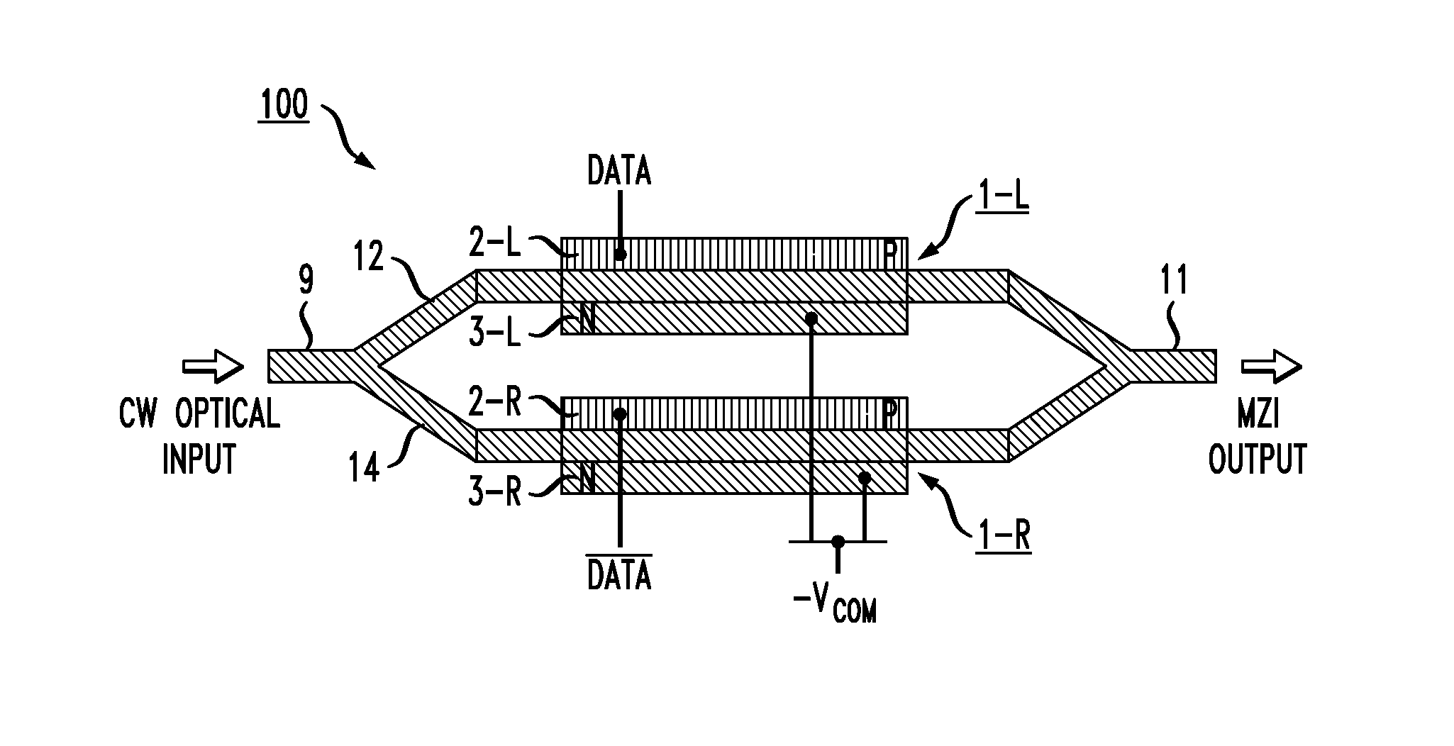
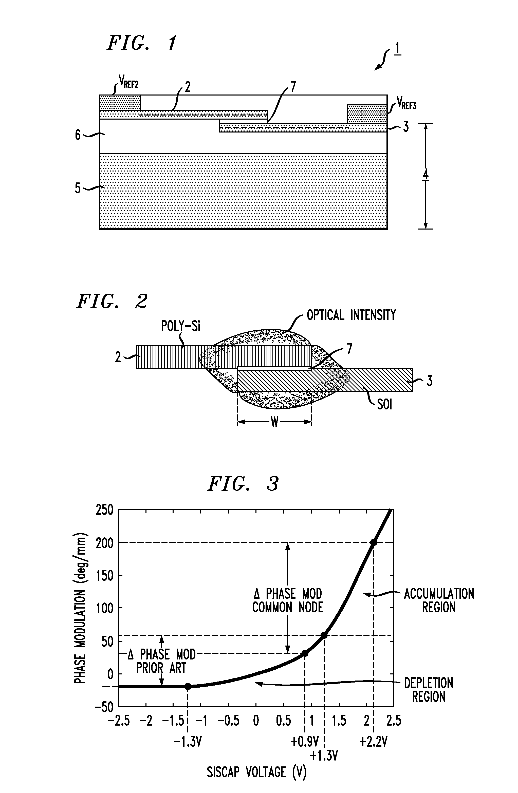
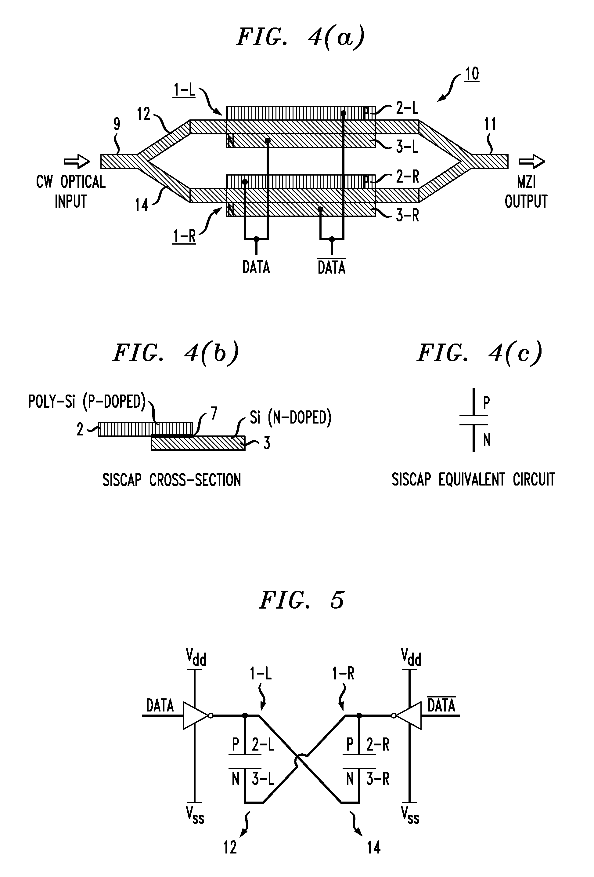
[0034]Prior to describing the utilization of “common node” biasing for improved modulation efficiency and chirp control in a silicon-based optical modulator, it is considered helpful to provide an understanding of the operation of a prior art silicon-based optical modulator in greater detail. FIG. 4(a) is a simplified block diagram of an exemplary prior art Mach Zehnder Interferometer (MZI) 10 comprising an input waveguide section 9 that splits into a pair of separate, parallel waveguiding arms 12 and 14. The opposite ends of waveguiding arms 12 and 14 are thereafter re-combined to form an output waveguide section 11. As shown, waveguiding arms 12 and 14 each contain a silicon-based phase modulating device 1 as discussed above in association with FIG. 1. In particular, waveguiding arm 12 contains a modulating device 1-L (comprising a polysilicon region 2-L and SOI region 3-L), and waveguiding arm 14 contains a modulating device 1-R (comprising a polysilicon region 2-R and SOI region...


PUM


Abstract

A silicon-based optical modulator exhibiting improved modulation efficiency and control of “chirp” (i.e., time-varying optical phase) is provided by separately biasing a selected, first region of the modulating device (e.g., the polysilicon region, defined as the common node). In particular, the common node is biased to shift the voltage swing of the silicon-based optical modulator into its accumulation region, which exhibits a larger change in phase as a function of applied voltage (larger OMA) and improved extinction ratio. The response in the accumulation region is also relatively linear, allowing for the chirp to be more easily controlled. The electrical modulation input signal (and its inverse) are applied as separate inputs to the second region (e.g., the SOI region) of each arm of the modulator.

Description


Claims


Application Information

Patent Timeline
Owner CISCO TECH INC
Why Eureka
Try Eureka