Light Emitting Device, Electronic Device, and Method for Driving Pixel Circuit

Inactive Publication Date: 2010-12-30
SEIKO EPSON CORP
View PDF5 Cites 14 Cited by
  • Summary
  • Abstract
  • Description
  • Claims
  • Application Information

AI Technical Summary

Benefits of technology

[0014]According to a third aspect of the invention, a method for driving a pixel circuit that includes a light emitting element; a driving transistor that is connected to the light emitting element in series; a storage capacitor that is located between a gate of the driving transistor and a source of the driving transistor; and a selecting transistor that is located between the gate of the driving transistor and a signal line that corresponds to the pixel circuit, includes: after a writing period starts, setting a potential of a selection signal to a selection potential to turn on the selecting transistor and outputting a data potential to the signal line to cause a current corresponding to the data potential to flow in the driving transis

Problems solved by technology

In a light emitting device in which driving transistors control driving currents that are supplied to light emitting elements, there i

Method used


Image

  • Light Emitting Device, Electronic Device, and Method for Driving Pixel Circuit
  • Light Emitting Device, Electronic Device, and Method for Driving Pixel Circuit
  • Light Emitting Device, Electronic Device, and Method for Driving Pixel Circuit

Examples


Example

First Modified Example

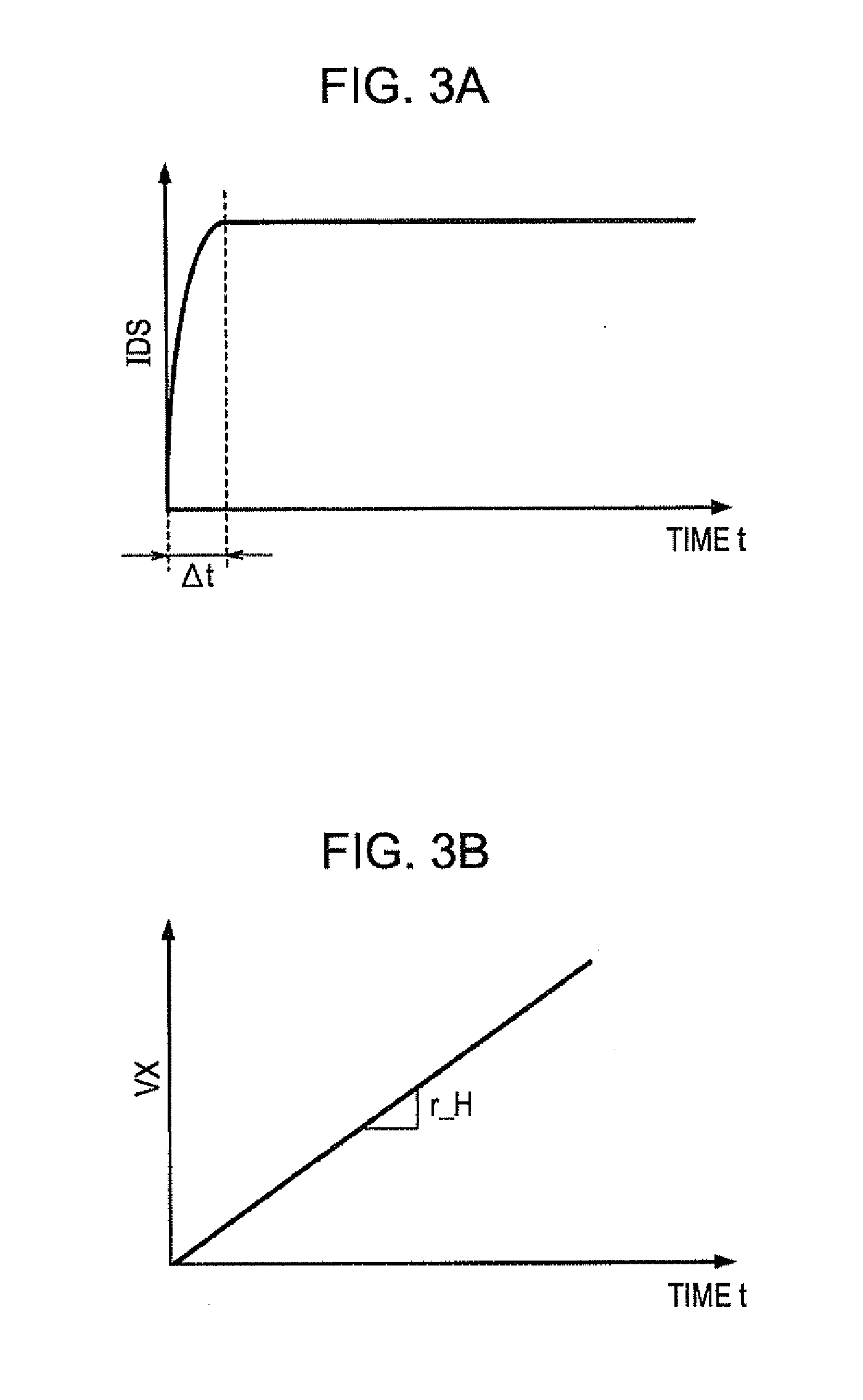
[0101]In the aforementioned embodiment, each of the data signals (data potentials VX) has the so-called ramp waveform, and the potential of each data signal is monotonically increased. When the specified gradation is high, the gradient of the potential of the data signal is steep. When the specified gradation is low, the gradient of the potential of the data signal is gentle. The selecting transistor TS is turned off during the time period when the potential of the data signal is monotonically increased. When a gradation for which the potential of the data signal is constant is specified, or when a gradation (low gradation) for which a change in the potential of the selected signal (scanning signal SWR) is approximately constant is specified, the selecting transistor TS does not need to be turned off during the period time when the potential of the data signal is monotonically increased.

Example

Second Modified Example

[0102]In the aforementioned embodiment, the potential of the scanning signal GWR[i] is set to the selection potential VSL at the start time is of the i-th writing period PWRT ((unit time period H[i]) that is included in the vertical scanning time period) and is linearly reduced over time at a constant rate for the i-th writing period PWRT (from the start time ts to the end time te). The change in the potential of the scanning signal GWR[i] is not limited to the aforementioned embodiment and may be arbitrary. In short, the potential of the scanning signal GWR[i] may be arbitrarily changed as long as the potential of the scanning signal GWR[i] changes over time for the writing period PWRT from the start time ts (when the potential of the scanning signal GWR[i] is set to the selection potential VSL) to the end time te.

[0103]In FIG. 11, when the maximum gradation Dmax is specified, the potential of the scanning signal may be arbitrarily set as long as the selectin...

Example

Fourth Modified Example

[0107]The conductivity type of each of the transistors (driving transistors TDR, selecting transistors TS, light emission control transistors TGEL, first switching elements SW1 and second switching elements SW2) is arbitrary. For example, the driving transistors TDR may be P-channel transistors. When the P-channel driving transistors TDR are used, the levels (high or low levels) of the voltages are reversed compared with the case in which the N-channel driving transistors TDR are used. However, operations of each P-channel driving transistor TDR are essentially the same as the operations of each N-channel driving transistor TDR described in the aforementioned embodiment and are not described in detail.

Fifth Embodiment

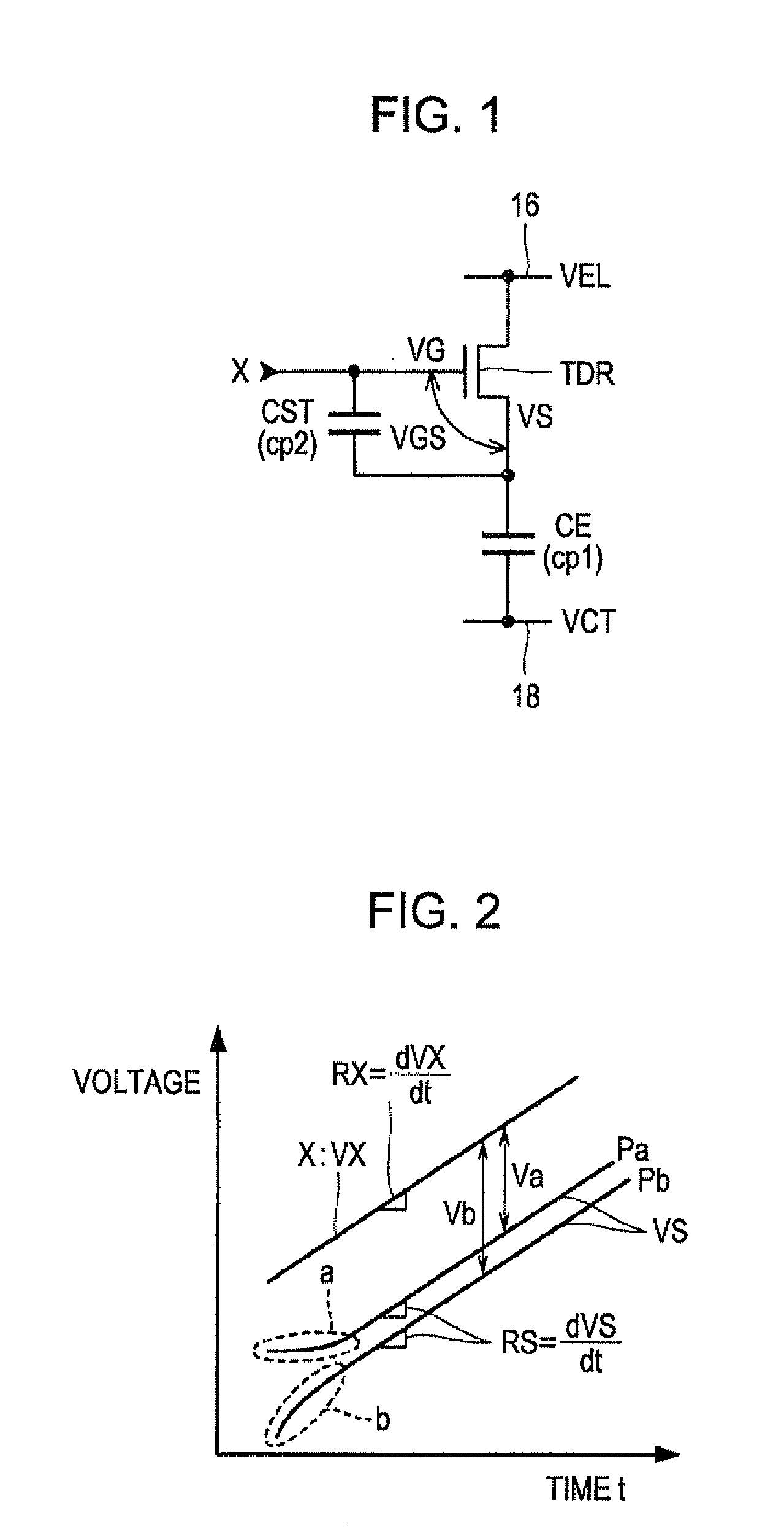
[0108]In the aforementioned embodiment, the amount of the driving current IDR that is to be supplied to the light emitting element E is determined on the basis of the rate RX of change of the data potential VX over time at the end time te of the w...


PUM


Abstract

A light emitting device includes: a pixel circuit; and a driving circuit that drives the pixel circuit, wherein the pixel circuit includes: a light emitting element; a driving transistor that is connected to the light emitting element in series; a storage capacitor that is located between a gate of the driving transistor and a source of the driving transistor; and a selecting transistor that is located between the gate of the driving transistor and a signal line that corresponds to the pixel circuit, after a writing period starts, the driving circuit sets a potential of a selection signal to a selection potential to turn on the selecting transistor and outputs a data potential to the signal line to cause a current corresponding to the data potential to flow in the driving transistor, the selection signal being to be supplied to the gate of the selecting transistor, the data potential being changed over time, and after the driving circuit sets the potential of the selection signal to the selection potential and outputs the data potential, the driving circuit changes, from the selection potential, the potential of the selection signal over time until the end time of the writing period to turn off the selecting transistor and thereby stop supply of the data potential and sets, to a rate corresponding to a gradation specified for the pixel circuit, a rate of change of the data potential at the time when the supply of the data potential to the driving transistor is stopped.

Description

BACKGROUND[0001]1. Technical Field[0002]The present invention relates to a technique for driving a light emitting element such as an organic electroluminescence (EL) element.[0003]2. Related Art[0004]In a light emitting device in which driving transistors control driving currents that are supplied to light emitting elements, there is a problem that electric characteristics of the driving transistors vary (or are different from a target value or the elements vary). JP-A-2007-310311 discloses a technique that compensates for a variation in a threshold voltage of a driving transistor and a variation in mobility of the driving transistor (and a variation in the amount of a driving current) by setting a voltage that is applied across the gate and source of the driving transistor to the threshold voltage and changing the set voltage on the basis of gradation.SUMMARY[0005]However, the variation in the amount of the driving current is effectively compensated for by the technique described i...

Claims


Application Information

Patent Timeline
IPC IPC(8): G09G5/00
CPCG09G3/3233G09G2300/043G09G2300/0819G09G2300/0861G09G2310/0251G09G2300/0852
Inventor ISHIGURO, HIDETOYATABE, SATOSHI
Owner SEIKO EPSON CORP
Why Eureka
Try Eureka