Strain relaxation using metal materials and related structures

a metal material and relaxation technology, applied in the direction of semiconductor devices, basic electric elements, electrical apparatus, etc., can solve the problems of limiting the thickness of the layers and/or the concentration of indium therein, limiting the thickness of the layers and/or the use of strained layers of semiconductor materials, and reducing the effect of cross-sectional separation

Active Publication Date: 2012-06-28
S O I TEC SILICON ON INSULATOR THECHNOLOGIES
View PDF1 Cites 12 Cited by
  • Summary
  • Abstract
  • Description
  • Claims
  • Application Information

AI Technical Summary

Benefits of technology

[0024]FIGS. 2A through 2C are simplified cross-sectional views of an intermediate structure that may be formed during embodiments of methods of the present invention;
[0025]FIGS. 3A through 3C are simplified cross-sectional views of an intermediate structure that may be formed during embodiments of methods of the present invention; and
[0026]FIGS. 4A through 4D are simplified cross-sectional views of an intermediate structure that may be formed during embodiments of methods of the present invention.

Problems solved by technology

The formation and use of strained layers of semiconductor material is limited because these strained layers may develop detrimental defects, such as dislocations, due to mismatch of the lattice parameters between adjacent materials.
However, as the concentration of dopant and the thickness of the semiconductor material are increased, preserving a crystal structure having low defect density may become increasingly difficult.
Mismatch in the crystal lattice structures of the adjacent layers of indium gallium nitride may induce strain within the crystal lattice of one or more of the layers, which may effectively limit the thickness of the layers and / or the concentration of indium therein.
Lattice strain is more problematic (e.g., in terms of obtaining good device performance) in indium gallium nitride device layers having higher indium content and increased thicknesses.
The presence of such lattice strain in a semiconductor material may be undesirable for a number of reasons.
For example, the presence of lattice strain in a semiconductor material may result in an increased density of defects (e.g., lattice dislocations) in the semiconductor material, undesirable morphology at the surface of the semiconductor material, and may even result in the formation of cracks in the semiconductor material.
Furthermore, the presence of lattice strain in a semiconductor material may facilitate the onset of undesirable separation of material phases within the semiconductor material.
Forming an indium gallium nitride seed layer on the surface of an engineered substrate in such a manner that the indium gallium nitride seed layer has a lattice parameter that will match that of an indium gallium nitride device layer to be formed thereover may be difficult to reach.
However, the concentration of boron and / or phosphorus may change over time as these impurities react with water or other atmospheric compounds.
As a result, it may be difficult to determine and maintain a desired concentration of boron and / or phosphorus and, thus, a consistent flow rate of BPSG during fabrication of indium gallium nitride device layers over BPSG material.
The use of such insulating BPSG materials may therefore prevent vertical current flow through engineered substrates comprising BPSG materials and thereby may limit the design and optimization of device structures formed on such engineered substrates.

Method used


Image

  • Strain relaxation using metal materials and related structures
  • Strain relaxation using metal materials and related structures
  • Strain relaxation using metal materials and related structures

Examples


embodiment 1

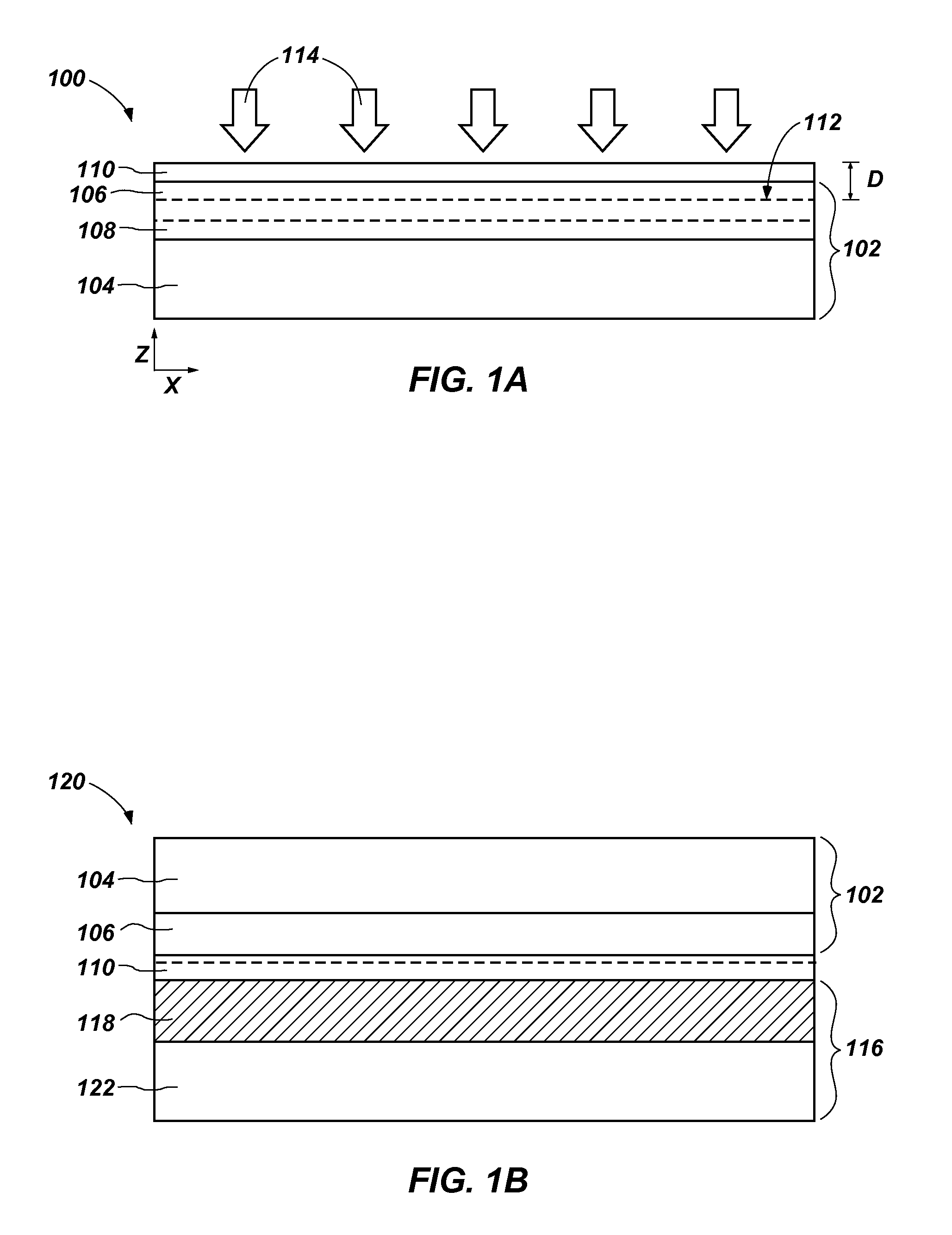
[0092] A method of fabricating a semiconductor structure, comprising: forming a metal material over a III-V type semiconductor material and deforming the metal material to relax the III-V type semiconductor material

[0093]Embodiment 2: The method of Embodiment 1, wherein deforming the metal material to relax the III-V type semiconductor material comprises deforming the metal material to reduce compressive strain in a III-V type semiconductor material comprising indium gallium nitride.

[0094]Embodiment 3: The method of Embodiment 1, wherein deforming the metal material to relax the III-V type semiconductor material comprises deforming the metal material to reduce tensile strain in a III-V type semiconductor material comprising aluminum gallium nitride.

[0095]Embodiment 4: The method of any one of Embodiments 1 through 3, wherein deforming the metal material to relax the III-V type semiconductor material comprises heating the metal material.

[0096]Embodiment 5: The method of any one of Em...

embodiment 8

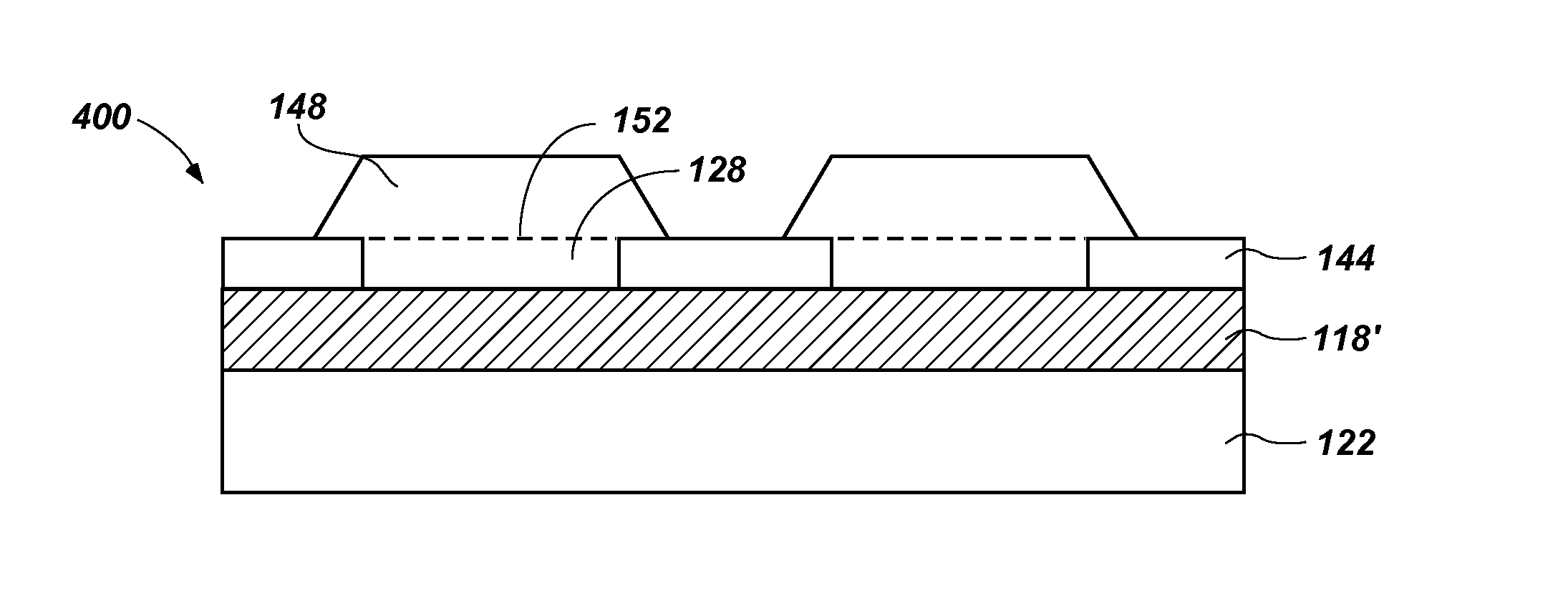
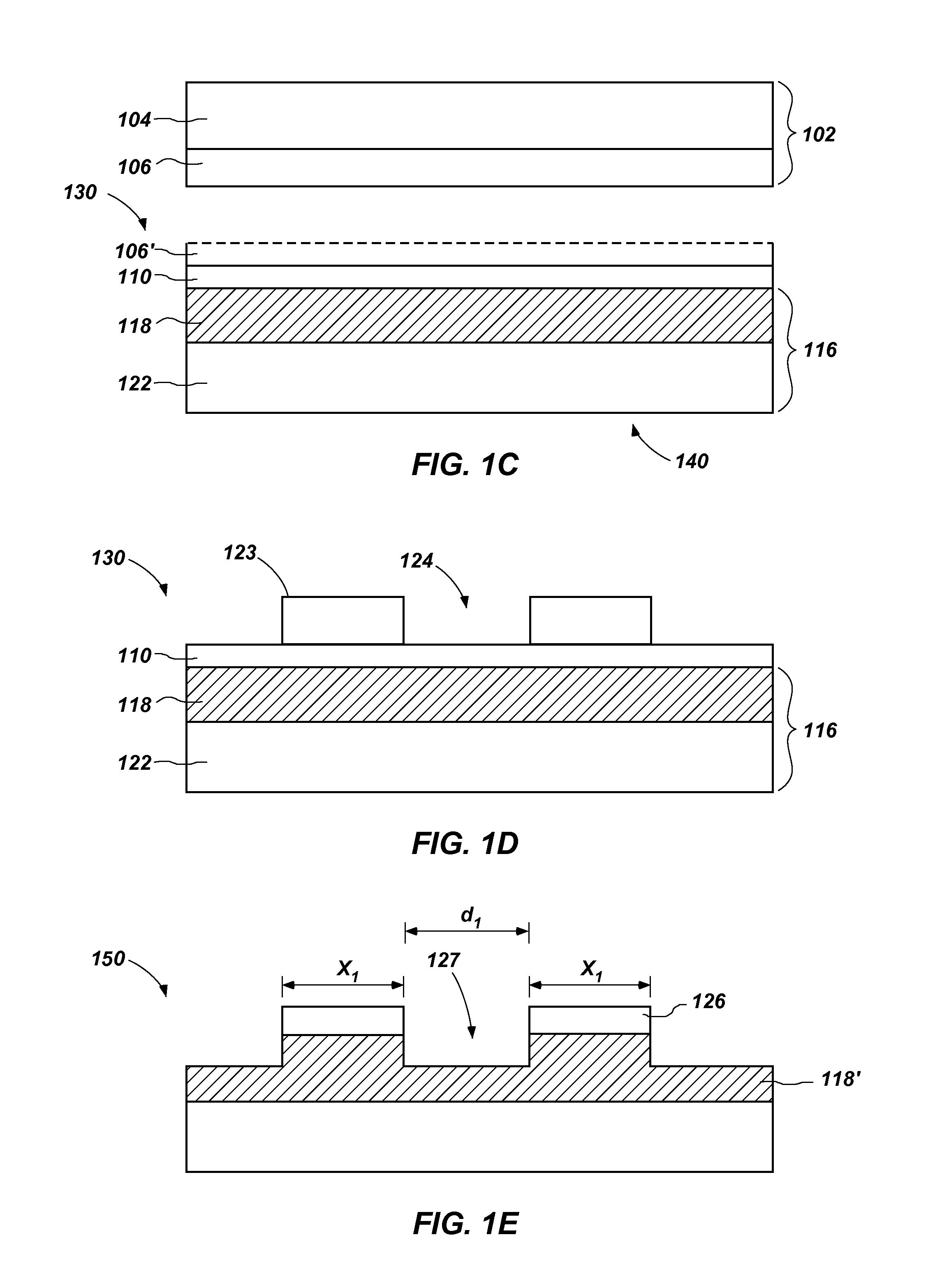
[0099] A method of fabricating a semiconductor structure, comprising: removing a portion of each of a semiconductor material and a metal material overlying a substrate to form a plurality of openings; heating the metal material to alter a ductility thereof; depositing another semiconductor material over the remaining portions of the semiconductor material; and removing a portion the metal material from between each of the remaining portions of the semiconductor material.

embodiment 9

[0100] The method of Embodiment 8, wherein removing a portion of each of a semiconductor material and a metal material overlying a substrate to form a plurality of openings comprises forming the plurality of openings to extend through the semiconductor material and partially into the metal material

[0101]Embodiment 10: The method of Embodiment 8 or Embodiment 9, heating the metal material to alter a ductility thereof occurs simultaneously with depositing another semiconductor material over the remaining portions of the semiconductor material.

[0102]Embodiment 11: The method of any one of Embodiments 8 through 10, heating the metal material to alter a ductility thereof comprises deforming a metal material comprising at least one of hafnium and zirconium.

[0103]Embodiment 12: The method of any one of Embodiments 8 through 11, further comprising heating the metal material to alter a ductility thereof after removing the portion the metal material between each of the remaining portions of t...


PUM

PropertyMeasurementUnit
temperatureaaaaaaaaaa
diametersaaaaaaaaaa
diametersaaaaaaaaaa

Abstract

Methods of fabricating semiconductor structures include forming a plurality of openings extending through a semiconductor material and at least partially through a metal material and deforming the metal material to relax a remaining portion of the semiconductor material. The metal material may be deformed exposing the metal material to a temperature sufficient it to alter (i.e., increase) its ductility. The metal material may be formed from one or more of hafnium, zirconium, yttrium and a metallic glass. Another semiconductor material may be deposited over the remaining portions of the semiconductor material, and a portion the metal material may be removed from between each of the remaining portions of the semiconductor material. Semiconductor structures may be formed using such methods.

Description

CROSS-REFERENCE TO RELATED APPLICATIONS[0001]The subject matter of this application is related to the subject matter of U.S. patent application Ser. No. 12 / 576,116 to Chantal Arena, titled “METHODS OF FORMING LAYERS OF SEMICONDUCTOR MATERIAL HAVING REDUCED LATTICE STRAIN, SEMICONDUCTOR STRUCTURES, DEVICES AND ENGINEERED SUBSTRATES INCLUDING SAME,” filed on Oct. 8, 2009, U.S. patent application Ser. No. 12 / 574,142 to Oleg Kononchuk, titled “RELAXATION OF A STRAINED MATERIAL LAYER WITH APPLICATION OF A STIFFENER,” filed on Oct. 6, 2009, U.S. patent application Ser. No. 12 / 563,953 to Letertre et al., titled “METHODS OF FORMING RELAXED LAYERS OF SEMICONDUCTOR MATERIALS, SEMICONDUCTOR STRUCTURES, DEVICES AND ENGINEERED SUBSTRATES INCLUDING SAME,” filed on Sep. 21, 2009, each of which is assigned to the Assignee of the present application, and the disclosure of each of which is incorporated by reference herein in its entirety.TECHNICAL FIELD[0002]The present invention generally relates to...

Claims


Application Information

Patent Timeline
Patent Type & Authority Applications(United States)
IPC IPC(8): H01L29/20H01L21/20
CPCH01L21/02002H01L29/2003H01L21/76254H01L21/185H01L21/242H01L21/02488H01L29/0684H01L21/02458
Inventor WERKHOVEN, CHRISTIAAN J.
Owner S O I TEC SILICON ON INSULATOR THECHNOLOGIES
Why Eureka
Try Eureka