Method of manufacturing a light emitting diode element

a technology of light-emitting diodes and manufacturing methods, which is applied in the direction of semiconductor/solid-state device manufacturing, electrical equipment, semiconductor devices, etc., can solve the problems of poor reliability and limit the heat dissipation efficiency

Active Publication Date: 2011-01-06
IND TECH RES INST
View PDF6 Cites 187 Cited by
  • Summary
  • Abstract
  • Description
  • Claims
  • Application Information

AI Technical Summary

Problems solved by technology

Therefore, the problem of current crowding occurs in the LEDs to limit the heat dissipation efficiency.
The gases with high press

Method used


Image

  • Method of manufacturing a light emitting diode element
  • Method of manufacturing a light emitting diode element
  • Method of manufacturing a light emitting diode element

Examples


Embodiment Construction

[0015]Reference will now be made in detail to the embodiments of the disclosure, examples of which are illustrated in the accompanying drawings. Wherever possible, the same reference numbers are used in the drawings and the description to refer to the same or like parts.

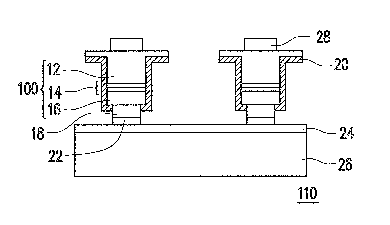
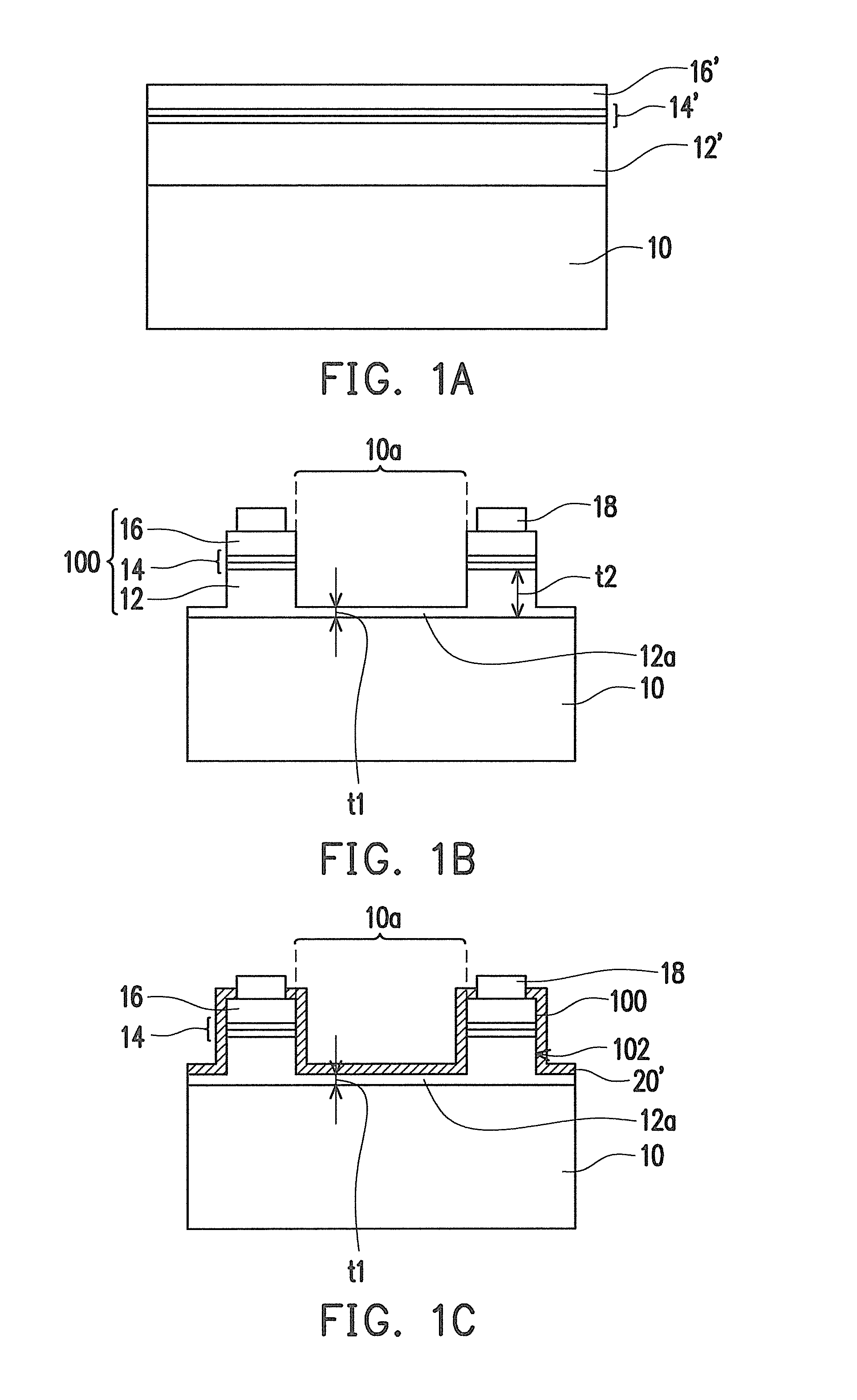
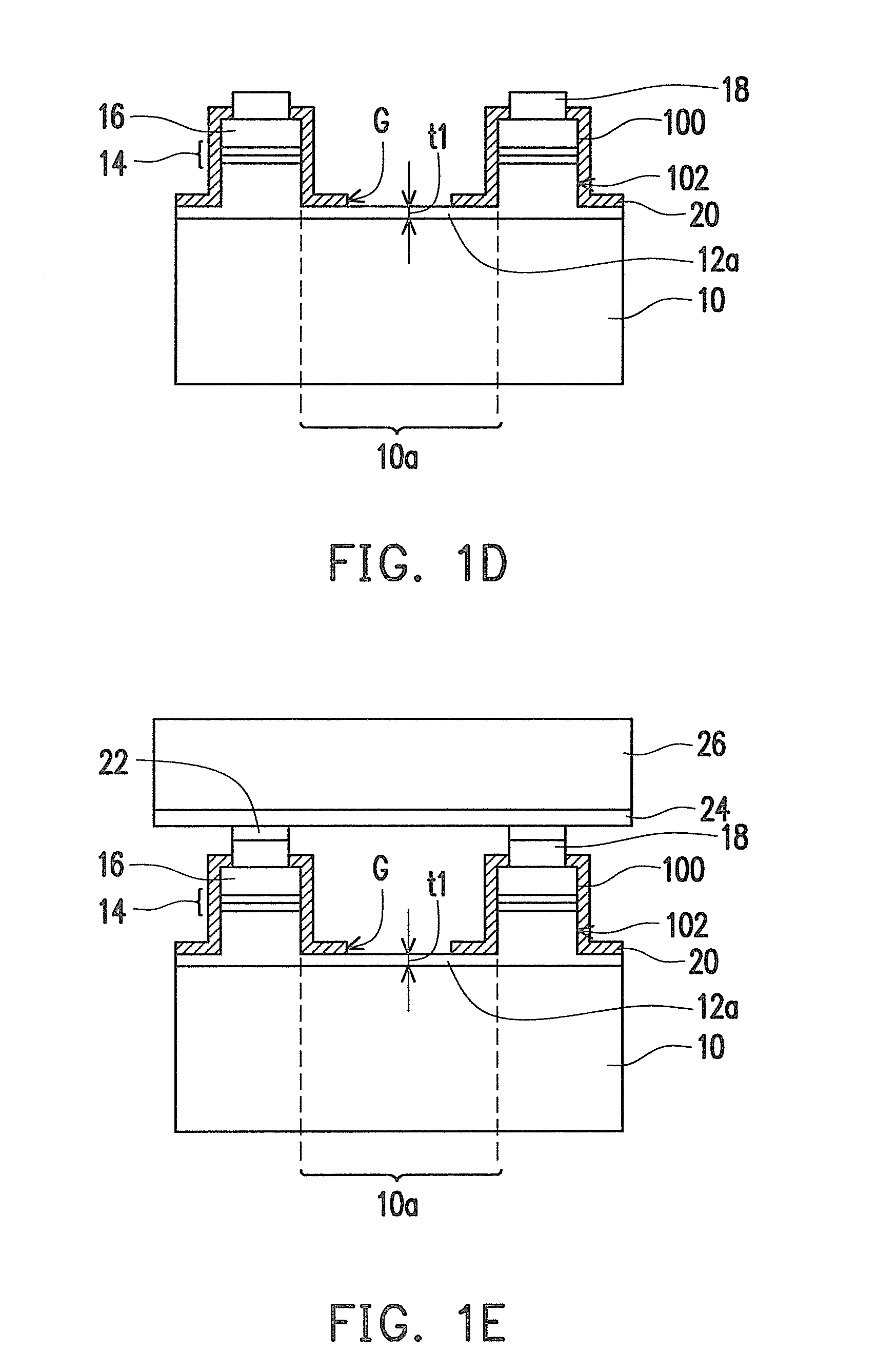
[0016]FIGS. 1A through 1G illustrate a method of manufacturing a light emitting diode (LED) element according to an embodiment. Referring to FIG. 1A, first, a first semi-conductor layer 12′, a light emitting layer 14′, and a second semi-conductor layer 16′ are sequentially formed on an epitaxy substrate 10. Herein, the epitaxy substrate 10 is, for example, a sapphire substrate, but in other embodiments the epitaxy substrate 10 may be other substrates suitable for manufacturing a light emitting diode element. In addition, the first semi-conductor layer 12′ may be an N type-semi-conductor layer and the second semi-conductor layer 16′ may be a p type-semi-conductor layer while the light emitting layer 14′ may be a Multi...


PUM


Abstract

A method of manufacturing a light emitting diode element is provided. A first patterned semi-conductor layer, a patterned light emitting layer, and a second patterned semi-conductor layer are sequentially formed on an epitaxy substrate so as to form a plurality of epitaxy structures, wherein the first patterned semi-conductor layer has a thinner portion in a non-epitaxy area outside the epitaxy structures. A passivation layer covering the epitaxy structures and the thinner portion is formed. The passivation layer covering on the thinner portion is partially removed to form a patterned passivation layer. A patterned reflector is formed directly on each of the epitaxy structures. The epitaxy structures are bonded to a carrier substrate. A lift-off process is performed to separate the epitaxy structures from the epitaxy substrate. An electrode is formed on each of the epitaxy structures far from the patterned reflector.

Description

CROSS-REFERENCE TO RELATED APPLICATION[0001]This application claims the priority benefit of U.S.A. provisional application Ser. No. 61 / 223,060 filed on Jul. 5, 2009. The entirety of the above-mentioned patent application is hereby incorporated by reference herein and made a part of specification.BACKGROUND[0002]1. Technical Field[0003]The disclosure generally relates to a method of manufacturing a light emitting diode (LED) element, in particular, to a method of manufacturing an LED element with increased yield rate.[0004]2. Description of Related Art[0005]Due to advantages of long lifetime, small volume, high shock absorption, low heat and power saving, LEDs have been widely used in household appliances and indicators or light sources of various instruments. In recent years, LEDs are developing towards rich colorfulness and high luminance, so that the applications of LEDs have been expanded to mega-size display board, traffic light, and so on. It can be expected that LEDs can subst...

Claims


Application Information

Patent Timeline
IPC IPC(8): H01L33/48H01L33/60
CPCH01L33/0079H01L33/44H01L33/405H01L33/20H01L33/0093
Inventor TSAY, JENQ-DARLIN, SUH-FANGCHANG, YU-HSIANGGUO, YIH-DERKUO, SHENG-HUEIKUO, WEI-HUNGLIU, HSUN-CHIH
Owner IND TECH RES INST
Why Eureka
Try Eureka