

Manufacturing method of semiconductor device
a manufacturing method and semiconductor technology, applied in semiconductor devices, semiconductor/solid-state device details, electrical devices, etc., can solve the problems of low accuracy in the manufacturing method and general insufficient accuracy of the dicing blade relative to the cutting position of an object to be processed
- Summary
- Abstract
- Description
- Claims
- Application Information
AI Technical Summary
Benefits of technology
Problems solved by technology
Method used
Image

Examples
Embodiment Construction
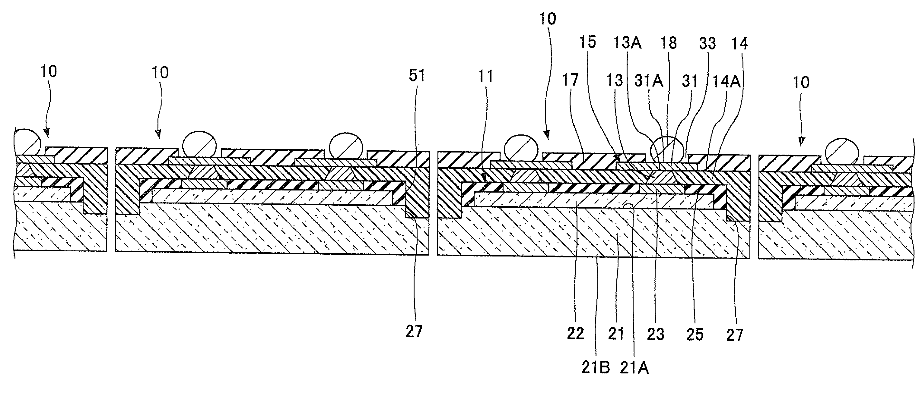
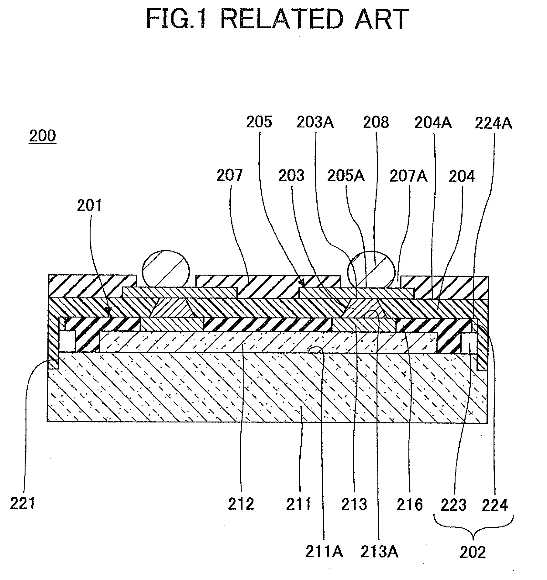
[0067]Hereinafter, numerical and alphabetical symbols typically designate as follows:[0068]10: Semiconductor device;[0069]11: Semiconductor chip;[0070]13: Internal connection terminal;[0071]13A: Connecting face;[0072]14: Insulating resin layer;[0073]15: Wiring pattern;[0074]17: Solder resist layer;[0075]18: External connection terminal;[0076]21: Semiconductor substrate;[0077]21A: Element forming face;[0078]22: Semiconductor element;[0079]22A, 25A, 41A: Upper surface;[0080]22B: Side surface;[0081]23: Electrode pad;[0082]23A: Connecting face;[0083]25: Protection film;[0084]27: Stepped portion;[0085]31: Externally connecting pad;[0086]31A: Terminal connecting face;[0087]33: Opening portion;[0088]35: Semiconductor substrate;[0089]35A, 35B, 53A: Surface;[0090]37: Check pattern;[0091]38: Check pattern body;[0092]39: Check pattern electrode;[0093]39A: Checking terminal connecting face;[0094]43: Through groove;[0095]45: Wet blast device;[0096]46: Jet nozzle;[0097]47: Liquid;[0098]48: Partic...
PUM
 Abstract
Description
Claims
Application Information