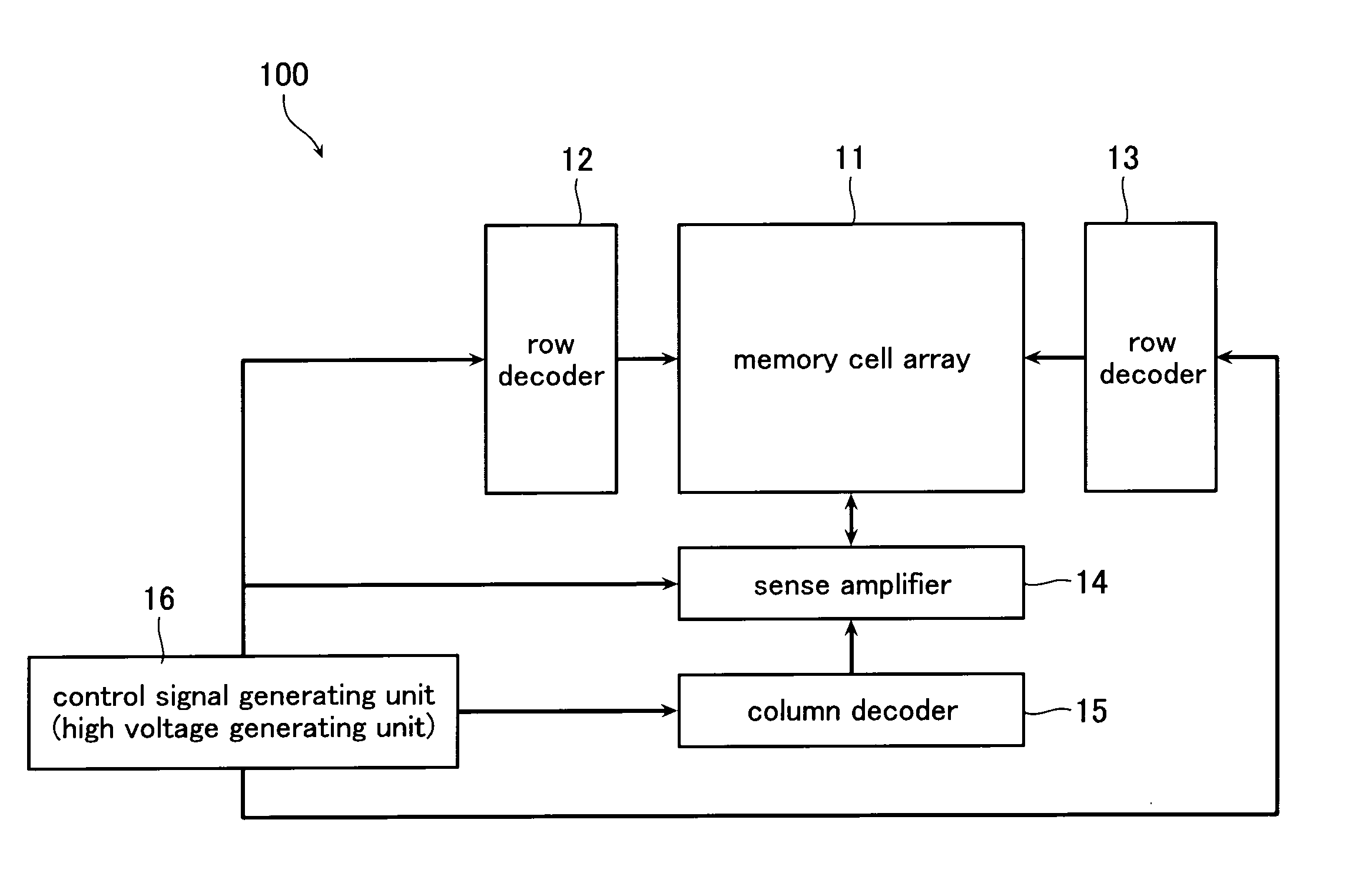
Nonvolatile semiconductor memory device
a non-volatile, semiconductor technology, applied in semiconductor devices, digital storage, instruments, etc., can solve the problems of euv steppers being expensive and unrealistic when considering costs, physical limitations such as those of withstanding voltage between elements, and the difficulty of miniaturization in cost and technology
- Summary
- Abstract
- Description
- Claims
- Application Information
AI Technical Summary
Problems solved by technology
Method used
Image


Examples
fourth embodiment
[0117]Next, a configuration of a nonvolatile semiconductor memory device in accordance with a fourth embodiment is described with reference to FIG. 8. FIG. 8 is a circuit diagram of the nonvolatile semiconductor memory device in accordance with the fourth embodiment. Note that in the fourth embodiment, identical symbols are assigned to configurations similar to those in the first through third embodiments and descriptions thereof are omitted.
[0118]The nonvolatile semiconductor memory device in accordance with the fourth embodiment includes a switch circuit SWa in place of the switch circuit SW. This switch circuit SWa has a structure substantially similar to that of the memory unit MU, as shown in FIG. 4. The switch circuit SWa controls electrical connection between the global bit line GBL and the local bit line LBL, similarly to the switch circuit SW in the first through third embodiments. The switch circuit SWa includes a memory string MSa, a drain side select transistor SDTra, an...
fifth embodiment
[0138]Next, a configuration of a nonvolatile semiconductor memory device in accordance with a fifth embodiment is described with reference to FIG. 10. FIG. 10 is a circuit diagram of the nonvolatile semiconductor memory device in accordance with the fifth embodiment. Note that in the fifth embodiment, identical symbols are assigned to configurations similar to those in the first through fourth embodiments and descriptions thereof are omitted.
[0139]The nonvolatile semiconductor memory device in accordance with the fifth embodiment has a switch circuit SWb that controls electrical connection between the global bit line GBL and the local bit line LBL similarly to the first through fourth embodiments. The switch circuit SWb has a configuration that is the configuration of the fourth embodiment with the memory string MSa omitted. That is, the switch circuit SWb is configured by a first select transistor SDTra and a second select transistor SSTra connected in series. These first select tr...
sixth embodiment
[0145]Next, a configuration of a nonvolatile semiconductor memory device in accordance with a sixth embodiment is described with reference to FIG. 12. FIG. 12 is a circuit diagram of the nonvolatile semiconductor memory device in accordance with the sixth embodiment. Note that in the sixth embodiment, identical symbols are assigned to configurations similar to those in the first through fifth embodiments and descriptions thereof are omitted.
[0146]The nonvolatile semiconductor memory device in accordance with the sixth embodiment includes a switch circuit SWc that differs from the previously mentioned switch circuits SW. As shown in FIG. 12, this switch circuit SWc controls electrical connection between the global bit line GBL and the local bit line LBL similarly to the first through fifth embodiments. However, the switch circuit SWc has a configuration that is the configuration of the fourth embodiment with the memory transistors MTra1-MTra8 removed. That is, the switch circuit SWc ...
PUM
 Abstract
Description
Claims
Application Information
 - R&D
- Intellectual Property
- Life Sciences
- Materials
- Tech Scout
- Unparalleled Data Quality
- Higher Quality Content
- 60% Fewer Hallucinations
Browse by: Latest US Patents, China's latest patents, Technical Efficacy Thesaurus, Application Domain, Technology Topic, Popular Technical Reports.
© 2025 PatSnap. All rights reserved.Legal|Privacy policy|Modern Slavery Act Transparency Statement|Sitemap|About US| Contact US: help@patsnap.com