Semiconductor device and method of fabricating the same

a technology of semiconductor devices and semiconductors, applied in semiconductor devices, semiconductor/solid-state device details, electrical apparatus, etc., can solve the problems of increasing electrical resistance at a connection, and the inability of contact plugs to electrically conduct through plugs

Active Publication Date: 2011-02-03
KK TOSHIBA
View PDF7 Cites 11 Cited by
  • Summary
  • Abstract
  • Description
  • Claims
  • Application Information

AI Technical Summary

Problems solved by technology

However, when the etching reaches the contact plug, there is a possibility that etching damage is generated on a bottom surface of the contact plug and the contact plug is not appropriately conn...

Method used


Image

  • Semiconductor device and method of fabricating the same
  • Semiconductor device and method of fabricating the same
  • Semiconductor device and method of fabricating the same

Examples


first embodiment

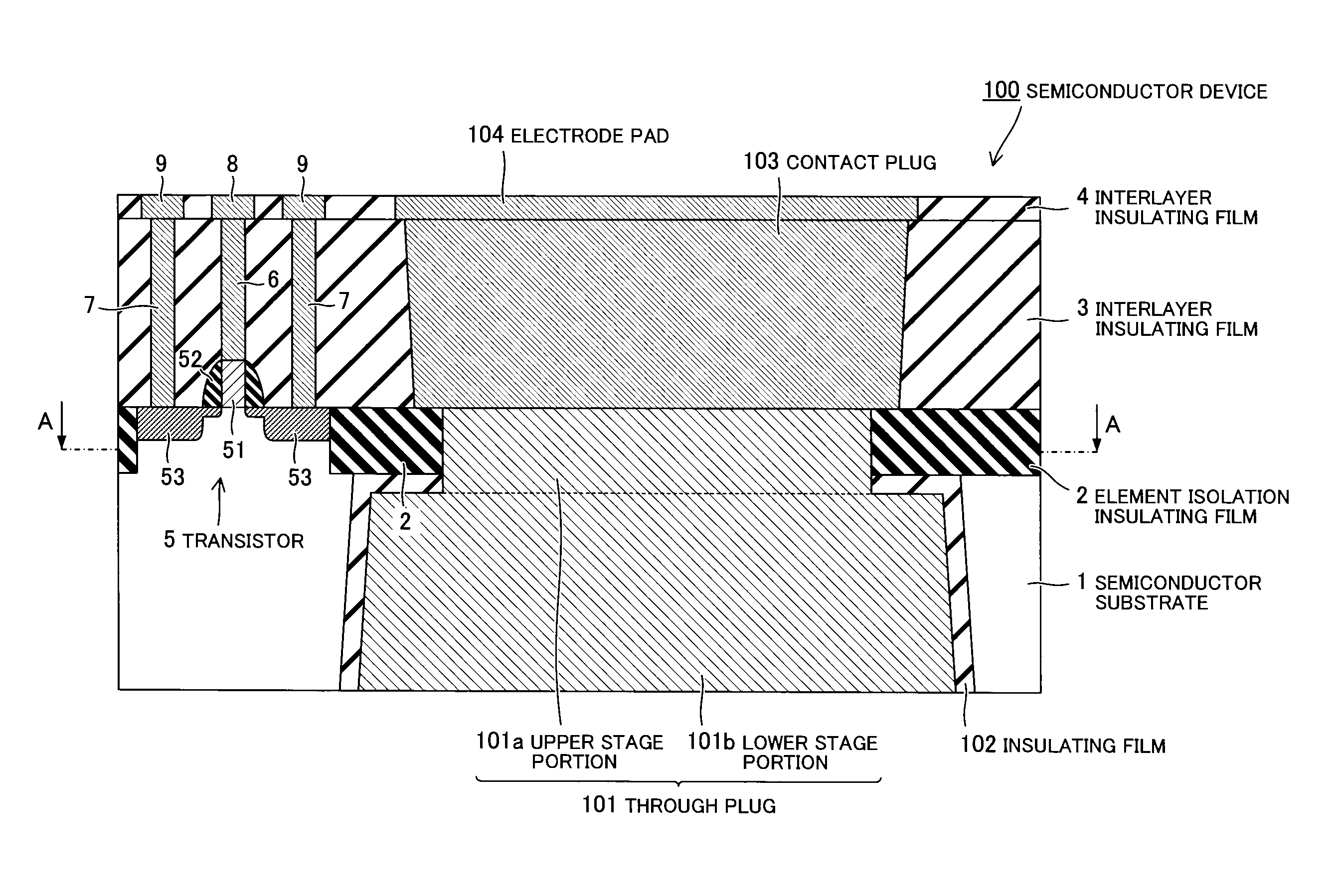
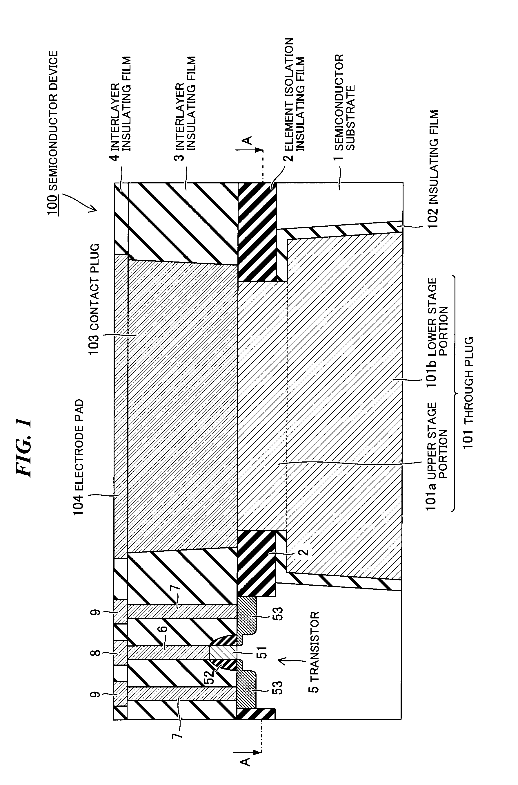
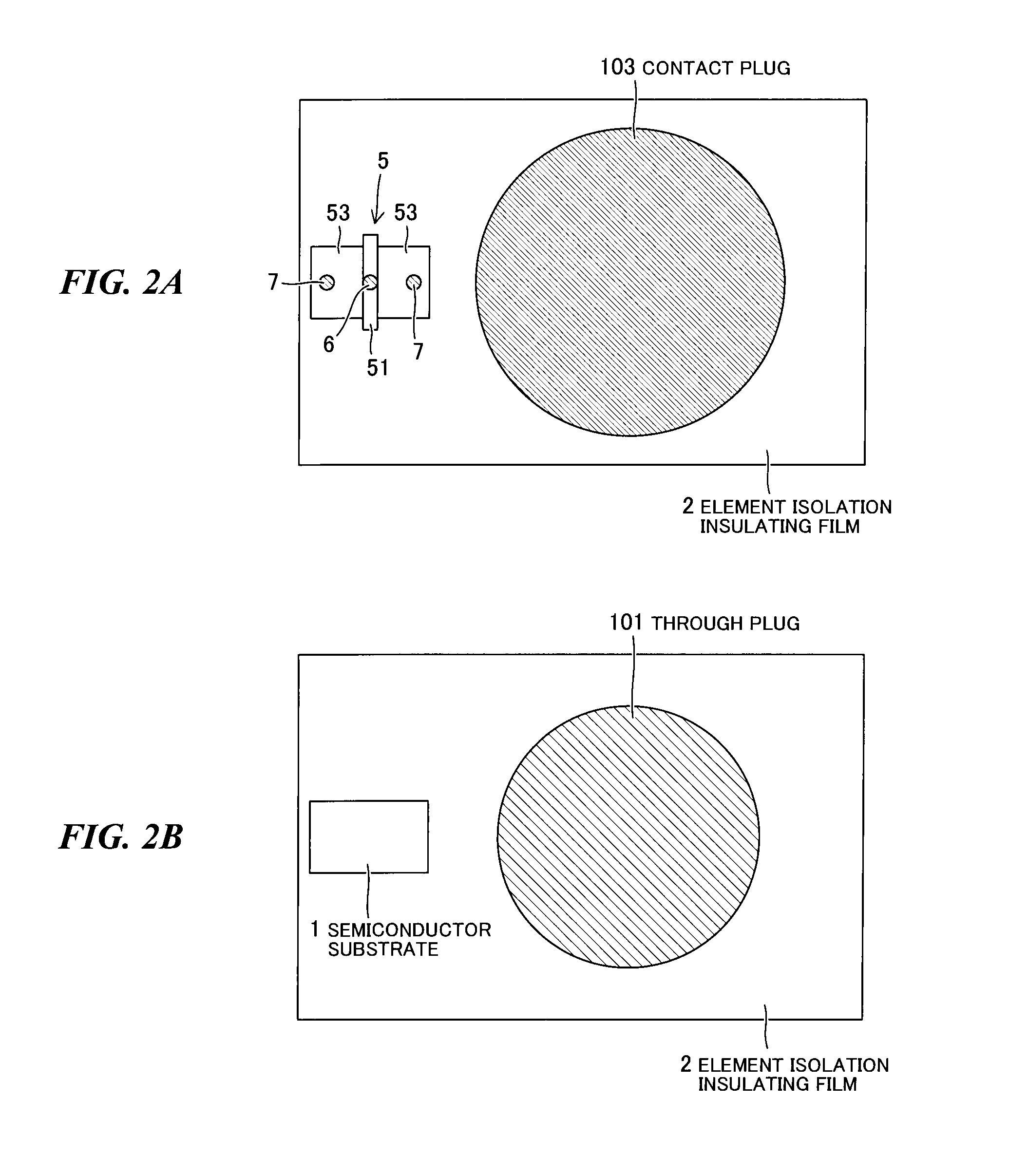
[0025]FIG. 1 is a cross sectional view of a semiconductor device 100 according to a first embodiment. In addition, FIG. 2A is a plan view of the semiconductor device 100 and FIG. 2B is across sectional view of the semiconductor device 100 taken on line A-A of FIG. 1. Note that, illustrations of below-described interlayer insulating films 3 and 4, wirings 8 and 9, an electrode pad 104 and a gate sidewall 52 are omitted in FIG. 2A.

[0026]A semiconductor device 100 has a transistor 5 formed on a semiconductor substrate 1 and electrically isolated from other elements by an element isolation insulating film 2, interlayer insulating films 3 and 4 formed on the semiconductor substrate 1, a through plug 101 penetrating the semiconductor substrate 1 from a back surface to a front surface, an electrode pad 104 formed in the interlayer insulating film 4, and a contact plug 103 formed in the interlayer insulating film 3 for connecting the through plug 101 to the electrode pad 104.

[0027]The semic...

second embodiment

[0064]The second embodiment is different from the first embodiment in that an interlayer insulating film is formed after formation of a dummy gate electrode in a region on an element isolation insulating film for forming a contact plug. Note that, the explanations will be omitted or simplified for the points same as the first embodiment.

[0065]An example of a method of fabricating a semiconductor device according to the present embodiment will be described hereinafter.

[0066]FIGS. 4A to 4C are cross sectional views showing processes for fabricating a semiconductor device according to a second embodiment.

[0067]Firstly, as shown in FIG. 4A, the element isolation insulating film 2, the transistor 5 and a dummy gate electrode 212 are formed on the semiconductor substrate 1, and then, the interlayer insulating film 3 is formed on the semiconductor substrate 1, the element isolation insulating film 2, the transistor 5 and the dummy gate electrode 212.

[0068]An insulating material is deposite...

third embodiment

[0077]The third embodiment is different from the first embodiment in patterns of a contact plug and an electrode pad. Note that, the explanations will be omitted or simplified for the points same as the first embodiment.

[0078]FIG. 5 is a cross sectional view of a semiconductor device 300 according to a third embodiment. In addition, FIG. 6A is a plan view of the semiconductor device 300 and FIG. 6B is across sectional view of the semiconductor device 300 taken on line B-B of FIG. 5. Note that, illustrations of below-described interlayer insulating films 3 and 4, wirings 8 and 9, an electrode pad 304 and a gate sidewall 52 are omitted in FIG. 6A.

[0079]A semiconductor device 300 has a transistor 5 formed on a semiconductor substrate 1 and electrically isolated from other elements by an element isolation insulating film 2, interlayer insulating films 3 and 4 formed on the semiconductor substrate 1, a through plug 301 penetrating the semiconductor substrate 1 from a back surface to a fr...


PUM


Abstract

A semiconductor device according to one embodiment includes: a semiconductor substrate; an element isolation insulating film embedded in the vicinity of a front surface of the semiconductor substrate; a through plug penetrating the semiconductor substrate from a back surface to the front surface so as to penetrate through the element isolation insulating film, and having a multi-stage structure comprising an upper stage portion and a lower stage portion, the upper stage portion having a region surrounded by the element isolation insulating film in the semiconductor substrate, the lower stage portion having a diameter larger than that of the upper stage portion; and a contact plug connected to an end portion of the through plug on the frond surface side of the semiconductor substrate for connecting a conductive member formed above the front surface side of the semiconductor substrate to the through plug.

Description

CROSS-REFERENCE TO RELATED APPLICATIONS[0001]This application is based upon and claims the benefit of priority from prior Japanese Patent Application No. 2009-175310, filed on Jul. 28, 2009, the entire contents of which are incorporated herein by reference.BACKGROUND[0002]A conventional semiconductor device is known in which a through plug (a through plug) is provided to a Si substrate for highly densifying wirings.[0003]There is a semiconductor device in which a through plug is connected to an upper wiring via a contact plug formed on a Si substrate. The semiconductor device, for example, is disclosed in JP-A 2007-123857. When a through plug is connected to an electrode pad formed on a Si substrate, there is a possibility that the electrode pad is removed due to overetching when a contact hole for the through plug is formed on the Si substrate, however, since the contact plug is thicker than the electrode pad, it is less likely to be removed even if etching reaches the contact plug...

Claims


Application Information

Patent Timeline
IPC IPC(8): H01L29/78H01L21/8234
CPCH01L21/76898H01L23/481H01L29/7833H01L2924/0002H01L2924/00
Inventor AKIYAMA, KAZUTAKA
Owner KK TOSHIBA
Why Eureka
Try Eureka