Image capture device, image capture apparatus, signal processing method, and program
a technology of image capture and image, which is applied in the field of image capture devices, image capture apparatuses, signal processing methods, and programs, can solve the problems of deteriorating image quality of images displayed, failure of added data, and difficulty in increasing the frame rate at which pixel data is transferred, so as to reduce the amount of pixel data output, reduce the transfer band, and reduce the time taken for pixel units
Inactive Publication Date: 2011-02-03
SONY CORP
View PDF3 Cites 15 Cited by
- Summary
- Abstract
- Description
- Claims
- Application Information
AI Technical Summary
Benefits of technology
[0039]With this arrangement, it is possible to reduce the time taken for the pixel units to output the pixel data.
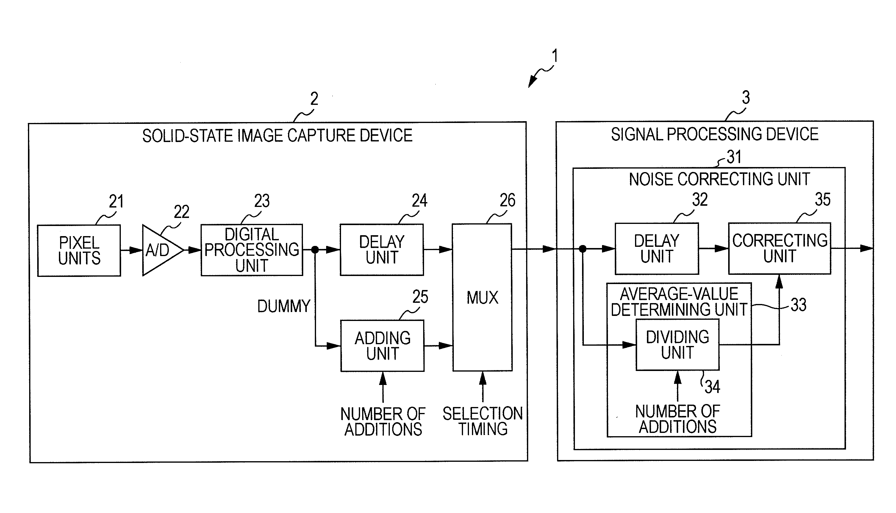
[0040]According to the present invention, either the second and third digital signals or the third digital signals are added a predetermined number of times. The added digital signals are divided by the number of additions to determine an average value of the signal levels of the digital signals, and the average value is output. This arrangement can reduce the amount of pixel data output from the pixel units and can reduce the transfer bands. As a result, there is an advantage in that the power consumption of the image capture device and the image capture apparatus can be reduced.
Problems solved by technology
Thus, it has been difficult to increase the frame rate at which the pixel data is transferred from the solid-state image capture device 101 to the signal processing device 105.
However, when the digital image signals are simply added, the resulting added data contains a failure, because of an influence of the image signal having the extraordinary signal level.
Even if a correction value is determined from such added data to correct the pixel data, the corrected pixel data has an erroneous value to cause deterioration of the image quality of an image displayed using digital image signals contained in the corrected pixel data.
When added data is generated even once, it is difficult to determine which part of the added data is affected by image signals output from the pixel having the pixel failure.
In such a case, noise correction can be performed with only low accuracy, which may cause deterioration of the image quality in many cases.
Method used
View moreImage
Smart ImageViewing Examples
Examples
first embodiment (
1. First Embodiment (Example in which Pixel Data Containing Added Data of Dummy Pixels is Transferred)
second embodiment (
2. Second Embodiment (Example in which Pixel Data Obtained by Dividing Added Data of Dummy Pixels into MSB and LSB is Transferred)
third embodiment (
3. Third Embodiment (Example in which Pixel Data Having Average Value of Dummy Pixels is Transferred)
Login to View More PUM
 Abstract
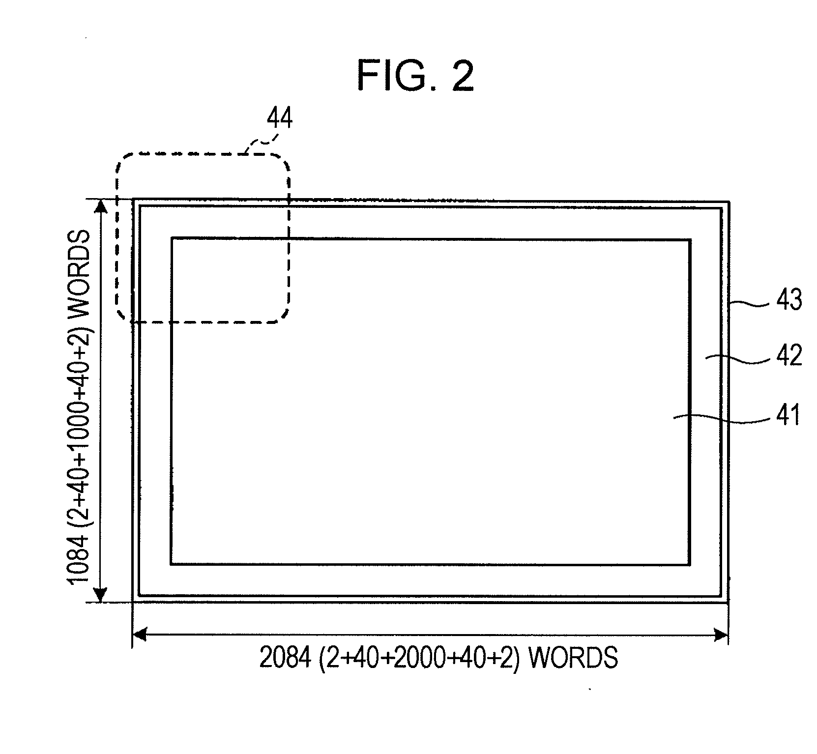
An image capture device includes: a digital processing unit that performs predetermined processing on pixel data containing first, second, and third digital signals obtained from pixel units having a valid pixel area for generating the first digital signals through photoelectrical conversion of incident image light, an optical black pixel area for generating the second digital signals, and a dummy pixel area for generating the third digital signals; an adding unit that adds the second-and-third-digital-signal-containing pixel data or the third-digital-signal-containing pixel data a predetermined number of times; a dividing unit that divides the added pixel data by the predetermined number of times, to determine an average value of levels of the digital signals; a delay unit that delays output of the first-to-third-digital-signal-containing pixel data by a predetermined amount of time; and a multiplexer that selects and outputs the first-to-third-digital-signal-containing pixel data or pixel data having the average value.
Description
BACKGROUND OF THE INVENTION[0001]1. Field of the Invention[0002]The present invention relates to an image capture device, an image capture apparatus, a signal processing method, and a program which are preferably applied to, for example, a case in which noise components superimposed on output signals of the image capture device are eliminated.[0003]2. Description of the Related Art[0004]Various technologies have been proposed in order to correct noise components (particularly, dark current noise or low-frequency fixed-pattern noise in columns and lines) superimposed on image signals output from a solid-state image capture device. One example of a technology for noise correction using optical black pixels (hereinafter may be referred to as “OB pixels”) or dummy pixels for outputting pseudo image signals generated by only analog-to-digital conversion regardless of the presence / absence of pixels. Image signals output from those pixels are read pixel by pixel in the same manner as valid...
Claims
Login to View More Application Information
Patent Timeline
 IPC IPC(8): H04N5/228
CPCH04N5/365H04N5/361H04N25/633H04N25/671H04N25/673H04N25/63H04N25/67
Inventor TAMAOKI, AKIHIRO
Owner SONY CORP


