Static Memory Device with Five Transistors and Operating Method

a technology of static memory and transistors, applied in the field of integrated circuits, can solve problems such as general incompatibility of constraints

Active Publication Date: 2011-02-03
STMICROELECTRONICS SRL
View PDF4 Cites 17 Cited by
  • Summary
  • Abstract
  • Description
  • Claims
  • Application Information

AI Technical Summary

Benefits of technology

[0022]In yet an additional aspect, the present invention provides for a method of copying the content of a first line of a memory plane into a second line of the memory plane, the memory plane having at least one column of memory cells of the SRAM type comprising two cross-coupled inverters and a single access transistor, each memory cell being connected between two bit lines without access transistors, and having a control means configured to deliver a first control signal to a gate of the access transistor of a first memory cell of the column and a second control signal to a gate of the access transistor of a second memory cell of the column. This method includes connecting the bit lines of each column to a power supply voltage, and placing the memory cells of a first line of the column in a read mode and placing the memory cells of a second line in the column in a write mode.

Problems solved by technology

Now, all these constraints are generally incompatible with advanced technologies in which the power supply voltage is relatively low, for example the 45 nanometre technologies in which the power supply voltage is 1.1 volt.

Method used


Image

  • Static Memory Device with Five Transistors and Operating Method
  • Static Memory Device with Five Transistors and Operating Method
  • Static Memory Device with Five Transistors and Operating Method

Examples


Embodiment Construction

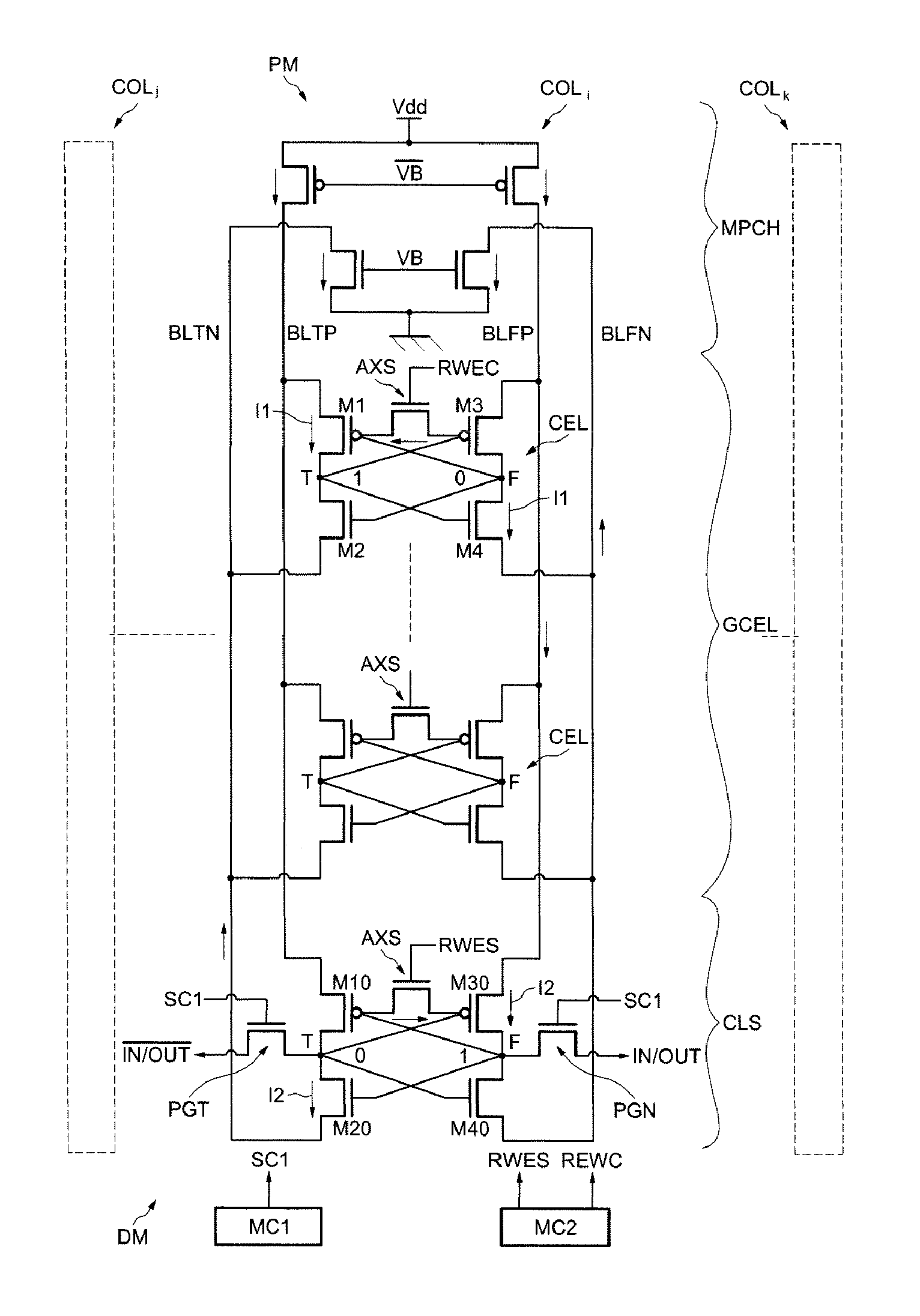
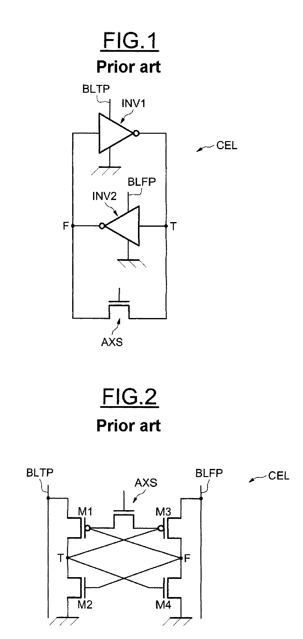
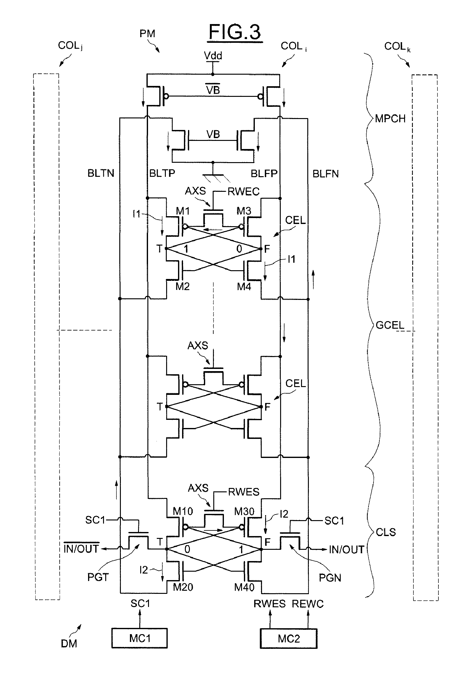
[0029]Before addressing specific embodiments in detail, a brief overview of the various embodiments, and potential advantages thereof, is provide. According to one embodiment, there is proposed a portless, five-transistor SRAM-type memory device that makes it possible to do away with the use of a current amplifier at the bottom of the column. There is also proposed, in particular, a dynamic current memory device, and therefore one with lower consumption. It is also proposed, in particular, to perform the write and read operations in the cells by means of a current, which does not require the charging and discharging of the bit lines in the write operations.

[0030]According to some illustrative embodiments, an SRAM-type memory device comprises a memory plane having at least one column of memory cells of the SRAM-type comprising two cross-coupled inverters and a single access transistor, each memory cell being connected between two lines of bits without access transistor. According to ...


PUM


Abstract

At the bottom of a column (COLi) of memory cells (CEL) of the SRAM type with five portless transistors, there is placed an additional cell (CLS), with a structure identical to the cells (CEL), which makes it possible to write and read a datum in a memory cell (CEL) of the column without using a read amplifier.

Description

[0001]This application claims priority to French Patent Application No. 09-55274, which was filed Jul. 28, 2009 and French Patent Application No. 10-50487, which was filed Jan. 26, 2010 both of which are incorporated herein by reference.TECHNICAL FIELD[0002]The invention relates to integrated circuits, and more particularly static memory devices, of the SRAM (Static Random Access Memory) type, with five transistors, said to be “portless,” also commonly referred to by those skilled in the art as “portless SRAMs.”BACKGROUND[0003]The memory cells of the portless, five-transistor SRAM type are well known to those skilled in the art. Notably worth citing is the article by Michael Wieckowski and Martin Margala entitled “Portless SRAM—A High-Performance Alternative to the 6T Methodology,” IEEE Journal of Solid-State Circuits, Volume 42, No. 11, November 2007, or the article by these same authors entitled “A Portless SRAM Cell Using Stunted Wordline Drivers,” IEEE 2008, pages 584-587.[0004]...

Claims


Application Information

Patent Timeline
Patent Type & Authority Applications(United States)
IPC IPC(8): G11C11/00G11C7/00
CPCG11C7/12G11C11/419G11C11/413G11C11/412
Inventor HAMOUCHE, LAHCENLAFONT, JEAN-CHRISTOPHE
Owner STMICROELECTRONICS SRL
Why Eureka
Try Eureka