Semiconductor device and fabricating method thereof

a technology of semiconductor devices and semiconductor devices, applied in the direction of semiconductor devices, semiconductor/solid-state device details, electrical apparatus, etc., can solve the problems of various parasitic components in the semiconductor device, esd may damage the internal elements of the semiconductor device, and the semiconductor device dies to malfunction

Active Publication Date: 2011-02-10
AMKOR TECH KOREA +1
View PDF18 Cites 81 Cited by
  • Summary
  • Abstract
  • Description
  • Claims
  • Application Information

AI Technical Summary

Problems solved by technology

When the semiconductor dies are stacked, it is difficult to supply electric power from a lower substrate to upper semiconductor dies, which causes the semiconductor dies to malfunction.
Since the ESD occurs at a high voltage, the ESD may damage the int...

Method used


Image

  • Semiconductor device and fabricating method thereof
  • Semiconductor device and fabricating method thereof
  • Semiconductor device and fabricating method thereof

Examples


Embodiment Construction

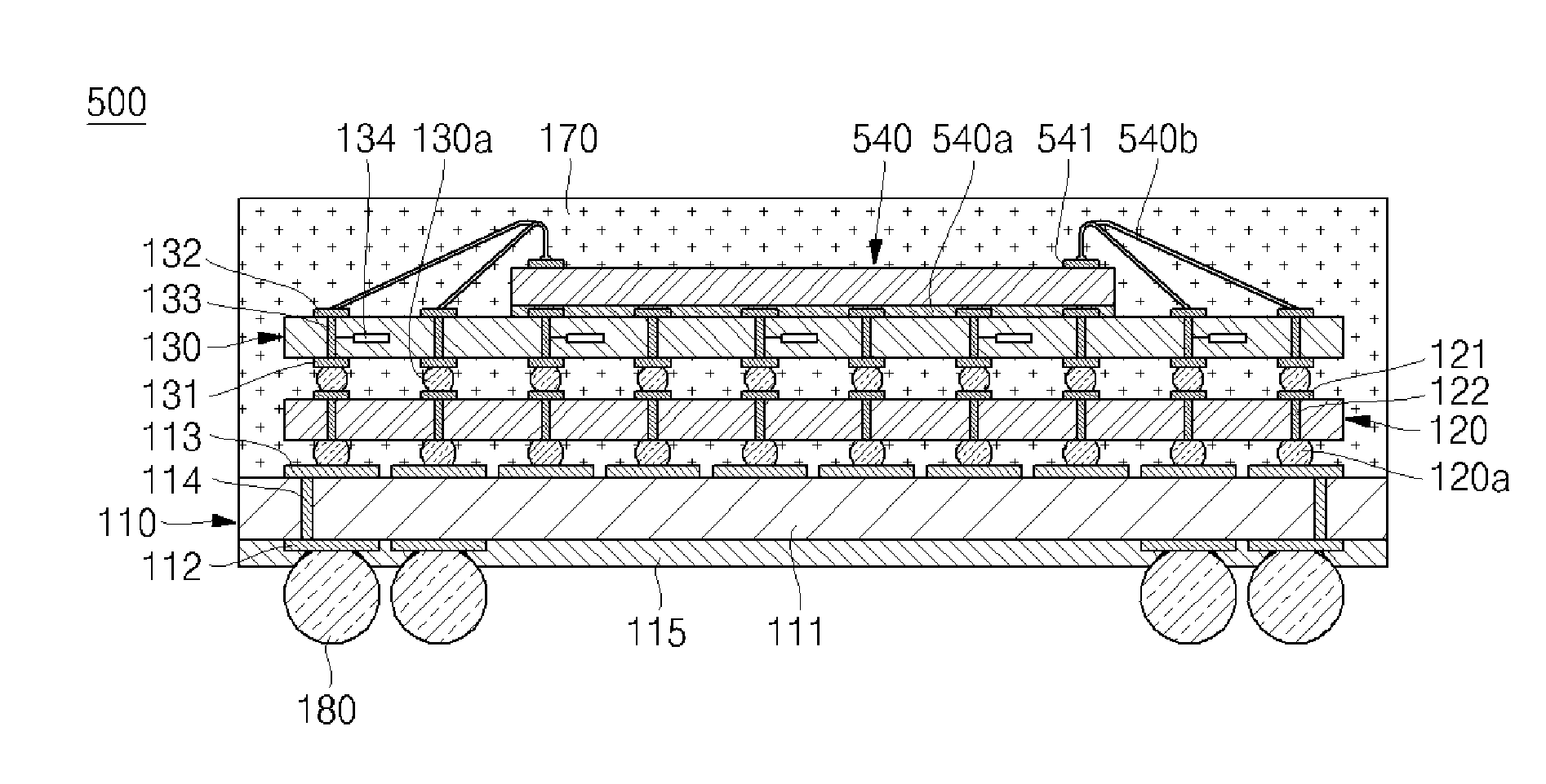
[0018]Referring to FIG. 1, a sectional view of a semiconductor device 100 according to an embodiment of the present invention is illustrated.

[0019]As illustrated in FIG. 1, the semiconductor device 100 according to an embodiment of the present invention includes a substrate 110, a first semiconductor die 120 formed on the substrate 110, an interposer 130 formed on the substrate 110, a second semiconductor die 140 formed on the interposer 130, an encapsulant 170 formed to surround the first semiconductor die 120, the interposer 130 and the second semiconductor die 140, and solder balls 180 formed under the substrate 110.

[0020]The substrate 110 provides a basis of the semiconductor device 100 according to an embodiment of the present invention. The substrate 110 includes lands 112 formed on the lower surface of an insulating layer 111, a plurality of conductive patterns 113 formed on the insulating layer 111, conductive vias 114 penetrating the insulating layer 111 to connect the land...


PUM


Abstract

A semiconductor device and a method of fabricating the same are disclosed. An interposer used for the semiconductor device includes integrated circuits therein to realize the functions of a decoupling capacitor, an ESD preventing circuit, an impedance matching circuit, and termination. Therefore, it is possible to improve the reliability of the operation of the semiconductor device.

Description

BACKGROUND OF THE INVENTION [0001]1. Field of the Invention[0002]The present invention relates to a semiconductor device including an interposer and a method of fabricating the same.[0003]2. Description of the Related Art[0004]Since recent semiconductor devices are required to have high capcities and high performance, in constituting one semiconductor device, a plurality of semiconductor dies are stacked in many cases. When the semiconductor dies are stacked, it is difficult to supply electric power from a lower substrate to upper semiconductor dies, which causes the semiconductor dies to malfunction.[0005]When static electricity is induced to the semiconductor device in the case where a human body touches the semiconductor device, the static electricity causes electrostatic discharge (ESD) to the semiconductor device. Since the ESD occurs at a high voltage, the ESD may damage the internal elements of the semiconductor device.[0006]In addition, there are various parasitic components...

Claims


Application Information

Patent Timeline
IPC IPC(8): H01L25/065H01L23/52H01L21/50
CPCH01L23/3128H01L2924/014H01L23/49827H01L23/49833H01L24/73H01L25/065H01L25/0657H01L2224/16145H01L2224/32225H01L2224/48091H01L2224/48227H01L2224/73265H01L2225/06506H01L2225/06541H01L2225/06551H01L2225/06572H01L2924/01029H01L2924/01082H01L2924/15311H01L2924/3011H01L23/49816H01L2924/01047H01L2924/19107H01L2224/85H01L24/85H01L24/48H01L2924/01033H01L2924/00014H01L2924/00H01L2924/00012H01L2224/06181H01L2224/06183H01L2224/13025H01L2224/16227H01L2224/17181H01L2224/73215H01L2924/19011H01L2924/19041H01L2924/19103H01L2924/19104H01L2924/12042H01L2924/14H01L2924/181H01L2224/45099H01L2224/05599
Inventor LEE, CHOON HEUNGBAE, KI CHEOLNA, DO HYUN
Owner AMKOR TECH KOREA
Why Eureka
Try Eureka