Constant Current Driving Circuit for Field Emission Device

a driving circuit and constant current technology, applied in the direction of instruments, light sources, discharge tubes cold cathodes, etc., can solve the problems of short circuit between the gate and the cathode electrode, the insulating layer may be damaged or broken, and the diode structure requires a high driving voltage, so as to increase the light emitting uniformity increase the stability and prolong the life of the field emission devi

Inactive Publication Date: 2011-02-17
KUMHO ELECTRIC INC
View PDF4 Cites 24 Cited by
  • Summary
  • Abstract
  • Description
  • Claims
  • Application Information

AI Technical Summary

Benefits of technology

[0015]A constant current driving circuit for a field emission device according to the present invention, a ground current of an anode electrode is measured in real time and the measured ground current is fedback to vary the frequency and duty ratio of a voltage applied to gate and cathode electrodes of a field emission device, thereby causing the ground current of the anode electrode to be constantly maintained. As a result, it is possible to increase the light emitting uniformity of the field emission device, to lengthen the life span of the field emission device, and increase the stability of the field emission device.

Problems solved by technology

However, the field emission device having a diode structure requires a high driving voltage and has a low light emitting efficiency.
At this time, in the conventional field emission device, over-current may be supplied due to external shock and malfunction of a driving circuit.
As a result, the insulating layer may be damaged or broken, and a short circuit between the gate and cathode electrodes may occur.
In addition, since current in the gate electrode is not constant, there is a problem in that a luminance difference may occur depending on a position of a screen of the field emission device.

Method used


Image

  • Constant Current Driving Circuit for Field Emission Device
  • Constant Current Driving Circuit for Field Emission Device
  • Constant Current Driving Circuit for Field Emission Device

Examples


Embodiment Construction

[0021]Hereinafter, the present invention will be described in detail with reference to the accompanying drawings.

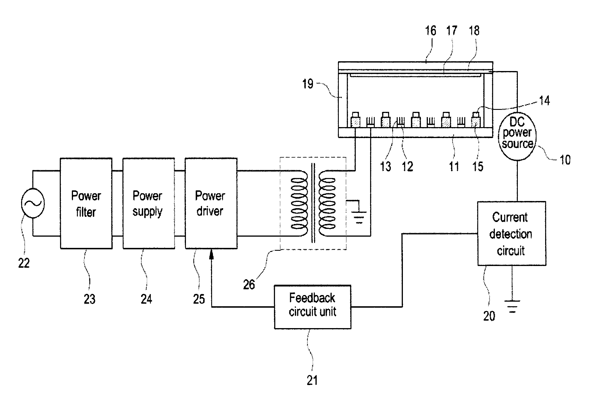
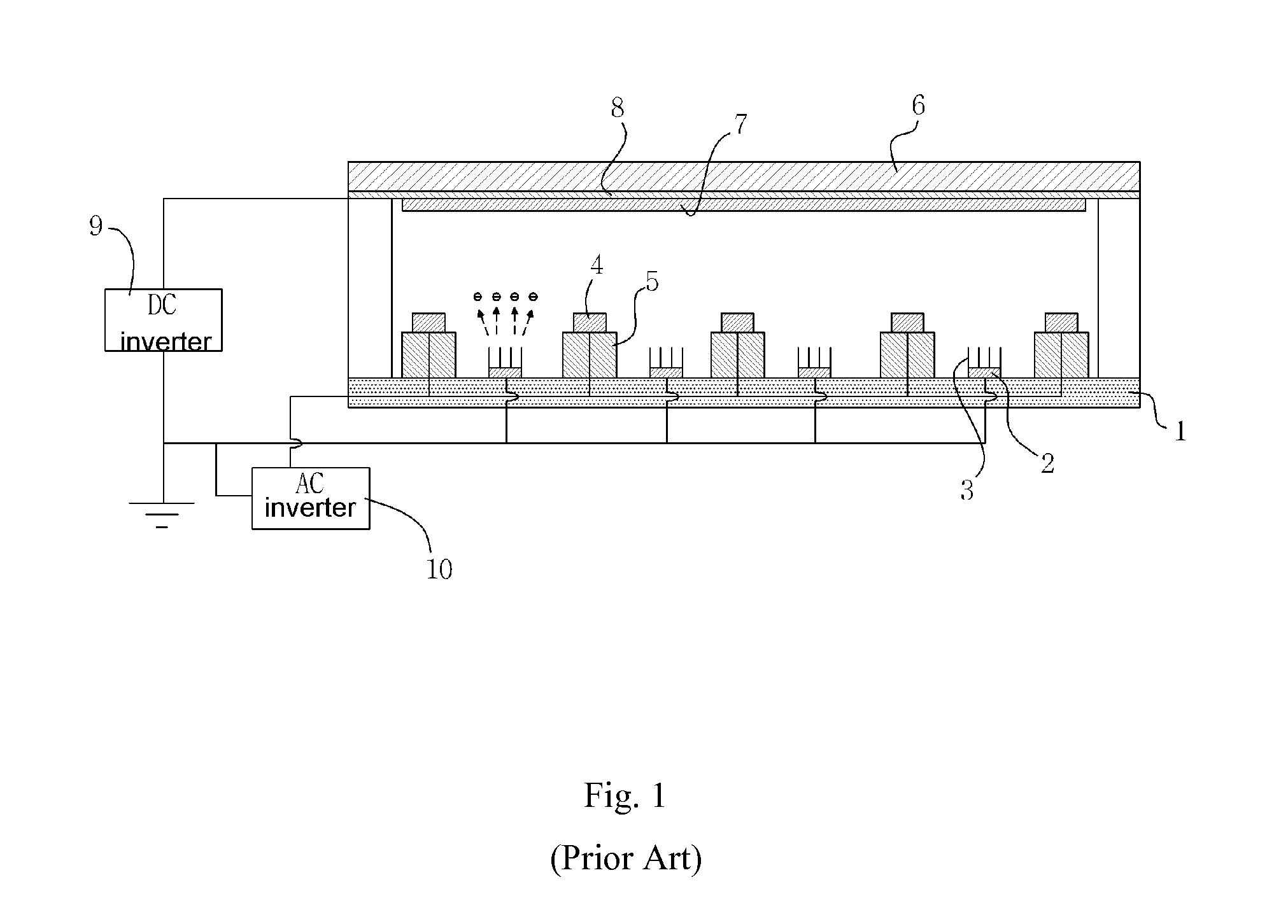
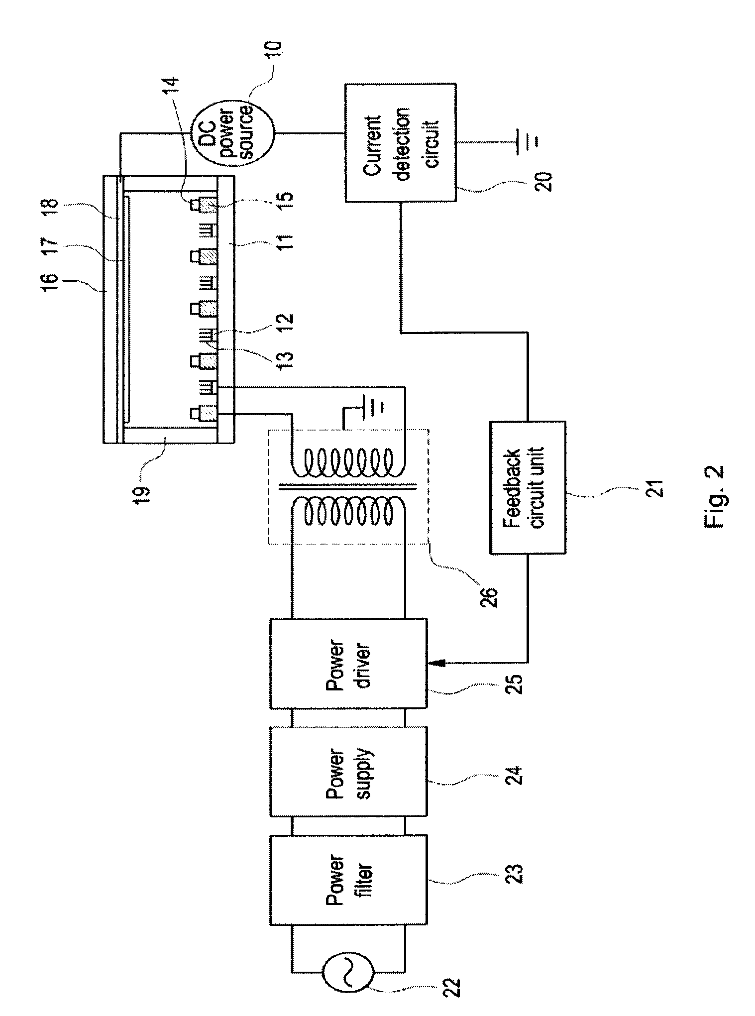
[0022]FIG. 2 is a view of a constant current driving circuit for a field emission device according to the present invention. Referring to FIG. 2, a lateral gate type field emission device configured such that a gate electrode is positioned at a side of a cathode electrode is driven by the constant current driving circuit according to the present invention.

[0023]First, the lateral gate type field emission device will be described. Front and rear substrates 16 and 11 are disposed opposite to each other while being spaced apart from each other at a predetermined distance. The front and rear substrates 16 and 11 are insulative substrates. Although glass, alumina, quartz or silicon wafers may be used as the front and rear substrates, glass substrates are preferably used in consideration of a manufacturing process and a large size.

[0024]At least one cathode electrode 12 made of...


PUM


Abstract

A constant current driving circuit for a field emission device has a ground current of an anode electrode measured in real time and the measured ground current is fedback to vary the frequency and duty ratio of a voltage applied to gate and cathode electrodes of the field emission device, thereby causing the ground current of the anode electrode to be constantly maintained. The field emission device has an anode electrode formed on a front substrate, gate and cathode electrodes formed on a rear substrate disposed opposite to the front substrate to be spaced apart from the front substrate by a predetermined distance, and an emitter formed on a top surface of the cathode electrode. The constant current driving circuit includes current detection circuit for detecting a ground current of the anode electrode; an input power unit for applying a driving AC voltage for emitting electrons from the emitter to the gate and cathode electrodes; and a feedback circuit unit for comparing the ground current of the anode electrode detected by the current detection circuit with a predetermined reference voltage to obtain a current variation and providing the input power unit with a frequency signal for varying a frequency of the driving AC voltage or a duty ratio signal for varying a duty ratio of the driving AC voltage in accordance with the current variation.

Description

RELATED APPLICATIONS[0001]This is a Continuation of PCT / KR2007 / 005465, filed Oct. 31, 2007, which published in English as WO 2009 / 057837A1 on May 7, 2009, and claims priority to KR 10-2007-0110595, also filed Oct. 31, 2007. The contents of the aforementioned PCT and Korean applications are incorporated by reference.FIELD OF THE INVENTION[0002]The present invention relates to a constant current driving circuit for a field emission device, and more particularly, to a constant current driving circuit for a field emission device, wherein a ground current of an anode electrode is measured in real time and the measured ground current is fedback to vary the frequency and duty ratio of a voltage applied to gate and cathode electrodes of a field emission device, thereby causing the ground current of the anode electrode to be constantly maintained.BACKGROUND[0003]Recently, the development of thin film displays using field emission has been actively conducted as lightweight and thin flat panel...

Claims


Application Information

Patent Timeline
Patent Type & Authority Applications(United States)
IPC IPC(8): H05B41/16
CPCG09G3/2014G09G3/22G09G2330/02G09G2320/029G09G2320/0233G09G3/20H01J1/30
Inventor KIM, KWANG BOKYANG, DONG WOOK
Owner KUMHO ELECTRIC INC
Why Eureka
Try Eureka