
Semiconductor device and on-vehicle ac generator

Inactive Publication Date: 2011-02-24
HITACHI LTD
View PDF4 Cites 15 Cited by
  • Summary
  • Abstract
  • Description
  • Claims
  • Application Information

AI Technical Summary

Benefits of technology

[0011]That is, in case of the above Japanese Patent No. 3152945, slight suppression of interface reactions can be expected by adding Ni, but interface reactions proceed at a high temperature of 200° C. or higher since the Cu6Sn5 and Cu3Sn compounds are always in contact with Cu and the Sn-based solder. Accordingly, the growth of the Cu—Sn compound continues and voids and other problems are generated at the interface. This results in lowered bonding reliability.
[0012]Meanwhile, in case of Japanese Unexamined Patent Publication No. 2002-280417 mentioned above, the intermetallic compound formed closest to the solder becomes a barrier layer between the Sn-based solder and the metal layer, and therefore great effect in suppressing interface reactions can be supposedly obtained. However, it is necessary to provide two layers: a first metal layer and a second metal layer, in advance on the bonded material, entailing the problems that the number of plating steps is increased; costs are increased by carrying out selective local plating; and formation of metal layers is difficult in case of a structure which prevents formation of electrodes. Moreover, the metal layer formed on the outermost surface of the bonding face needs to be reacted with Sn-based solder in bonding to provide a barrier layer. Therefore, when the metal layer formed on the outermost surface is thick, the unreacted metal layer on the outermost surface remains in bonding, which may create the problems that the effect of the barrier layer cannot be suffi

Problems solved by technology

However, prior art inventions have the problems mentioned below, and they do not have sufficient suppression on interface reactions, and have low bonding reliability.
In particular, it was found that suppression of interface reactions in a semiconductor device for on-vehicle AC generators (alternator) used at high temperatures by the prior art is difficult.
Accordingly, the growth of the Cu—Sn compound continues and voids and other problems are generated at the interface.
This results in lowered bonding reliability.
However, it is necessary to provide two layers: a first metal layer and a second metal layer, in advance on the bonded material, entailing the problems that the number of plating steps is increased; costs are increased by carrying out selective local plating; and formation of metal layers is difficult in case of a structure which prevents formation of electrodes.
Therefore, when the metal layer formed on the outermost surface is thick, the unreacted metal layer on the

Method used


Image

  • Semiconductor device and on-vehicle ac generator
  • Semiconductor device and on-vehicle ac generator
  • Semiconductor device and on-vehicle ac generator

Examples


Example

[0037]According to the present invention, an environmental friendly semiconductor device having heat resistance of 200° C. or higher can be provided.

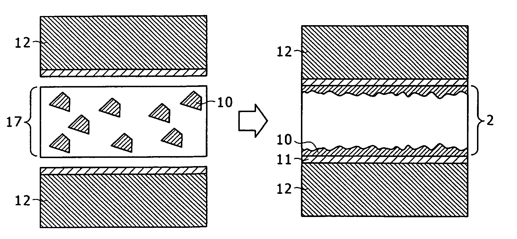
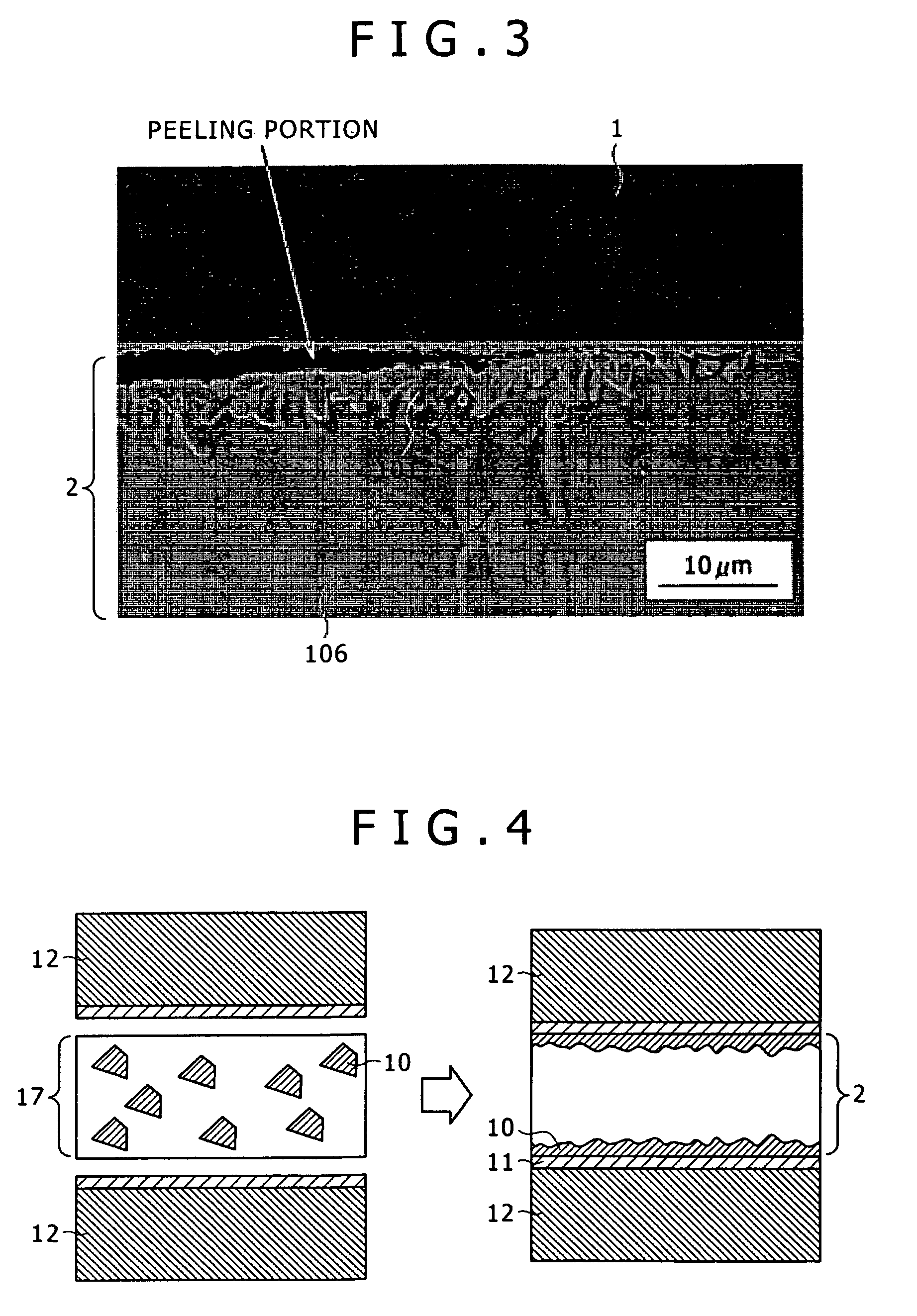
[0038]To begin with, the bonding material and bonding mechanism of the present invention will be described with reference to FIG. 4.

[0039]An example of the bonding material of the present invention an Sn-based solder foil 17 containing a phase 10 of a Cu—Sn compound (e.g., Cu6Sn5) at a temperature from room temperature to 200° C. By bonding bonded materials 12 on which a Ni-based plating 11 is formed using this solder foil 17, Cu6Sn5 phases 10 floating in the solder foil 17 as phases deposit or move onto the Ni-based platings 11, so that compound layers 10 mainly composed of a Cu—Sn compound (Cu6Sn5 phase) are formed. Herein, when the compound layers are formed, the Ni platings 11 are partly fused to form a (Cu,Nu)6Sn5 compound in some cases. In this case, the compound layers 10 become intermetallic compound layers containing at least o...


PUM


Abstract

An object of the present invention is to provide, at low costs, an environmental friendly bonding material for a semiconductor, having sustained bonding reliability even when used at a temperature as high as 200° C. or higher for a long period of time, the semiconductor device having a semiconductor element, a supporting electrode body bonded to a first face of the semiconductor element via a first bonding member, and a lead electrode body bonded to a second face of the semiconductor element supported by the supporting electrode body via a second bonding member, the semiconductor device having a Ni-based plating layer and an intermetallic compound layer containing at least one of Cu6Sn5 and (Cu,Ni)6Sn5 compounds at an interface between the supporting electrode body and the first bonding member, and having a Ni-based plating layer and an intermetallic compound layer containing at least one of Cu6Sn5 and (Cu,Ni)6Sn5 compounds at an interface between the lead electrode body and the second bonding member.

Description

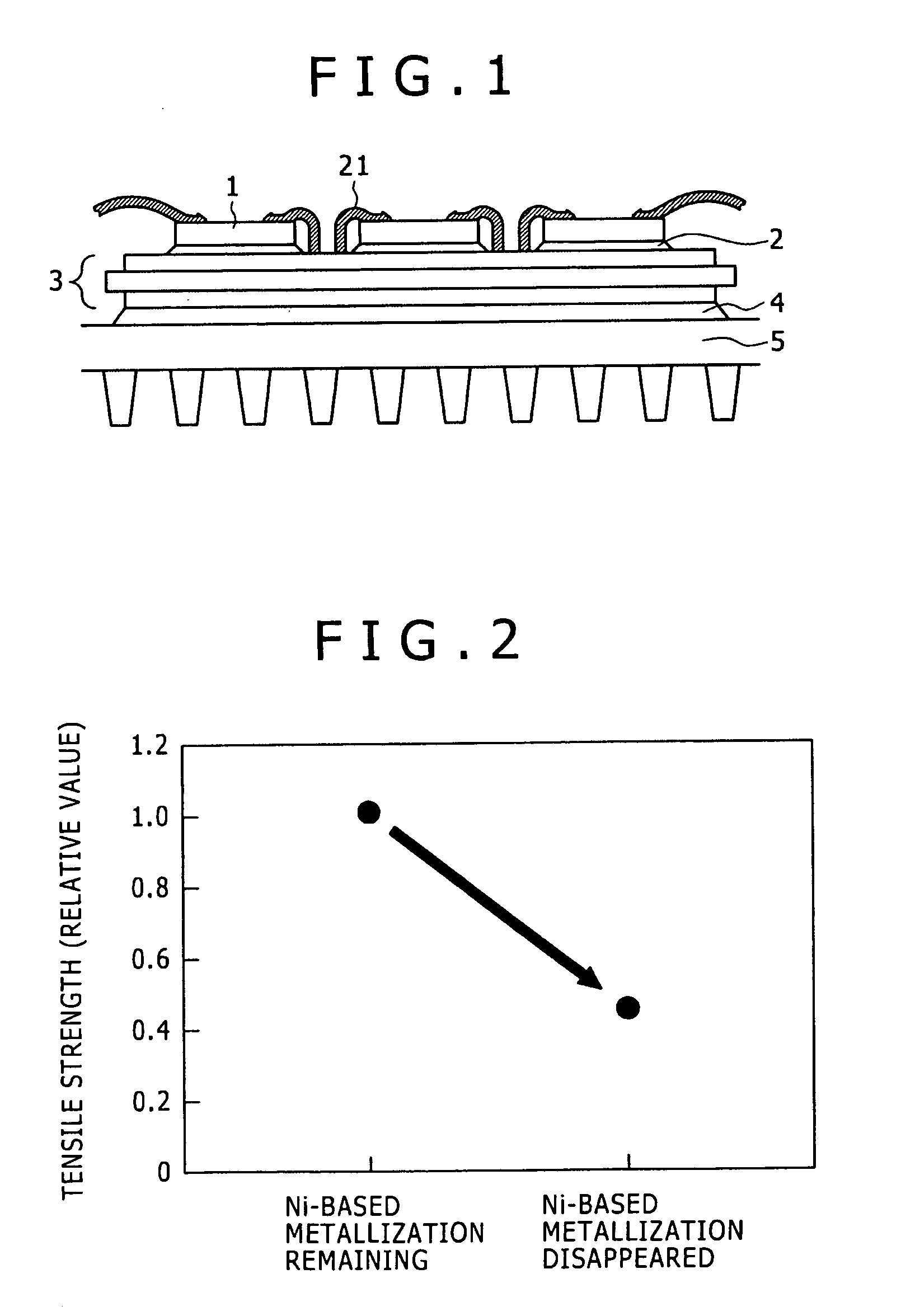
BACKGROUND OF THE INVENTION[0001](1) Field of the Invention[0002]The present invention relates to a semiconductor device and an on-vehicle AC generator.[0003](2) Description of the Related Art[0004]In power electronics products, as shown in FIG. 1, a hierarchical bonding in which a semiconductor element 1 is mounted on a substrate 3, bonded by a bonding member 2, and is further bonded to a supporting member 5 by a bonding member 4 is often provided. Accordingly, In the bonding of the semiconductor element 1, high-lead solders (melting point: about 300° C.) having low reactivity with components during fusing of solder and under high heat circumstances have been used in order to avoid the disappearance of a Ni-based metallization (not shown) formed on the supporting member 5 and the bonding face of the semiconductor element 1 for bearing bond strength. However, since the solders have high contents of lead of 85 mass % or higher, development of lead-free semiconductor devices has been ...

Claims


Application Information

Patent Timeline
IPC IPC(8): H01L23/482
CPCH01L23/488H01L2924/10253H01L24/27H01L24/32H01L24/33H01L24/45H01L2224/32225H01L2224/32507H01L2224/45124H01L2224/48227H01L2224/73265H01L2224/83101H01L2924/01005H01L2924/01012H01L2924/01013H01L2924/01014H01L2924/01015H01L2924/0102H01L2924/01029H01L2924/0103H01L2924/01033H01L2924/01042H01L2924/01046H01L2924/01047H01L2924/0105H01L2924/01074H01L2924/01075H01L2924/01078H01L2924/01079H01L2924/01082H01L2924/01322H01L2924/01327H01L2924/13055H01L2924/0132H01L24/29H01L24/48H01L2224/32245H01L2224/83455H01L2224/83805H01L2924/01006H01L2924/01023H01L2924/01024H01L2924/014H01L2924/0133H01L2224/29111H01L2924/15311H01L2924/01028H01L2224/48091H01L24/01H01L2924/00014H01L2924/00H01L2924/01032H01L2924/00012H01L2924/3512H01L2924/181H01L2924/00011H01L24/73H01L2224/83065H01L2224/2612H01L2224/83205
Inventor IKEDA, OSAMUMATSUYOSHI, SATOSHI
Owner HITACHI LTD
Learn More