

Semiconductor device, apparatus, and method for producing semiconductor device
- Summary
- Abstract
- Description
- Claims
- Application Information
AI Technical Summary
Benefits of technology
Problems solved by technology
Method used
Image

Examples
embodiment 1
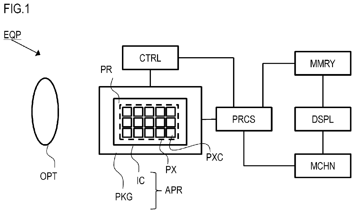
[0069]FIG. 1 is a schematic view illustrating a semiconductor device APR according to the present embodiment. The semiconductor device APR includes, in addition to a semiconductor device IC including a semiconductor layer 100 and a semiconductor layer 200, a package PKG for mounting the semiconductor device IC. In the present embodiment, the semiconductor device APR is a photoelectric conversion device. The semiconductor device IC has a pixel region PX in which pixel circuits PXC are arranged in a matrix and a peripheral region PR around the pixel region PX. Peripheral circuits can be provided in the peripheral region PR.
[0070]The semiconductor device APR is also provided in an apparatus EQP. Here, the apparatus EQP may include at least any one of an optical system OPT, a control device CTRL, a processing device PRCS, a display device DSPL, a storage device MMRY, and a mechanical device MCHN. The apparatus EQP will be described in detail hereinbelow.
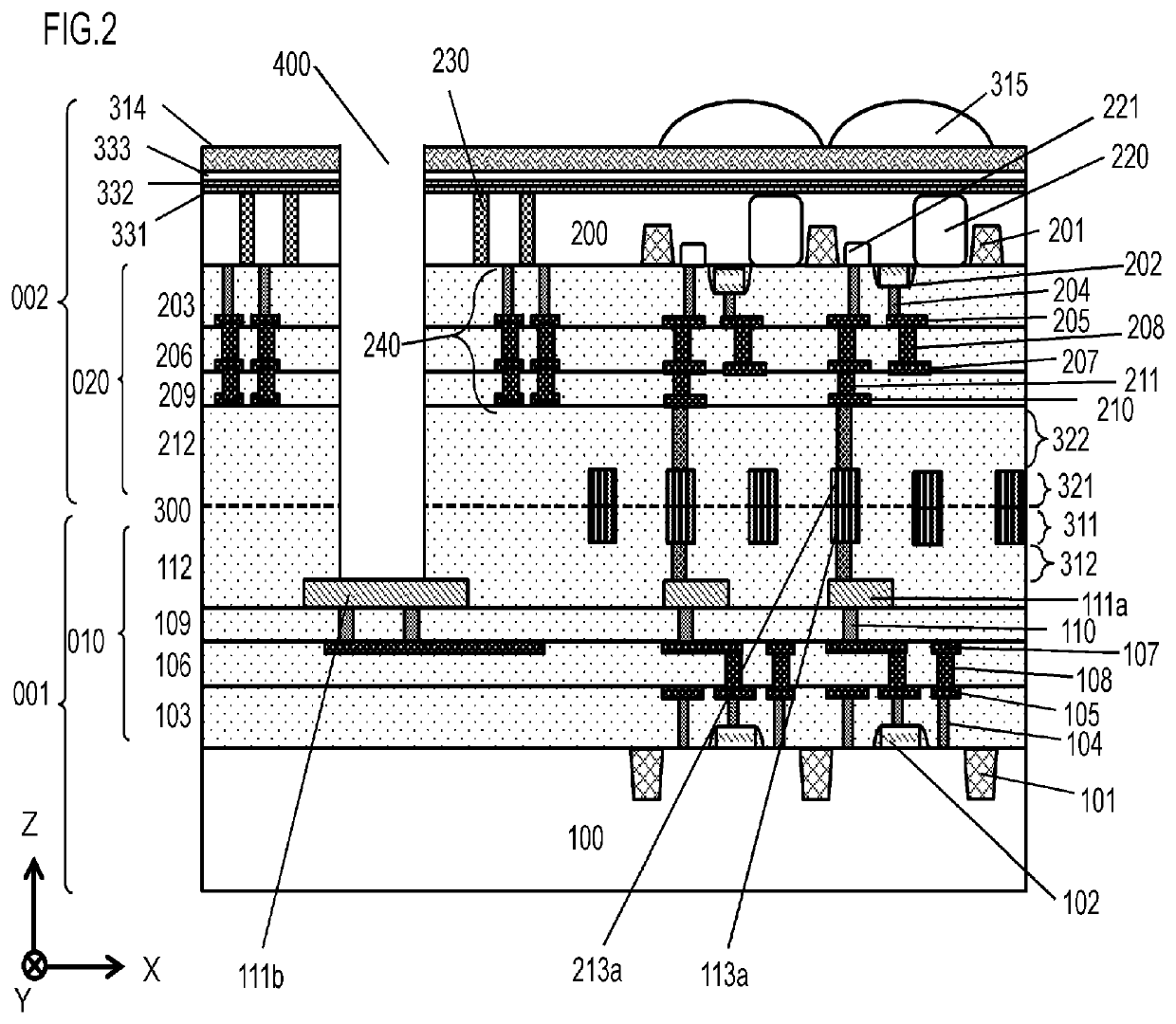
[0071]FIG. 2 is a cross-sectional...
modification example 1
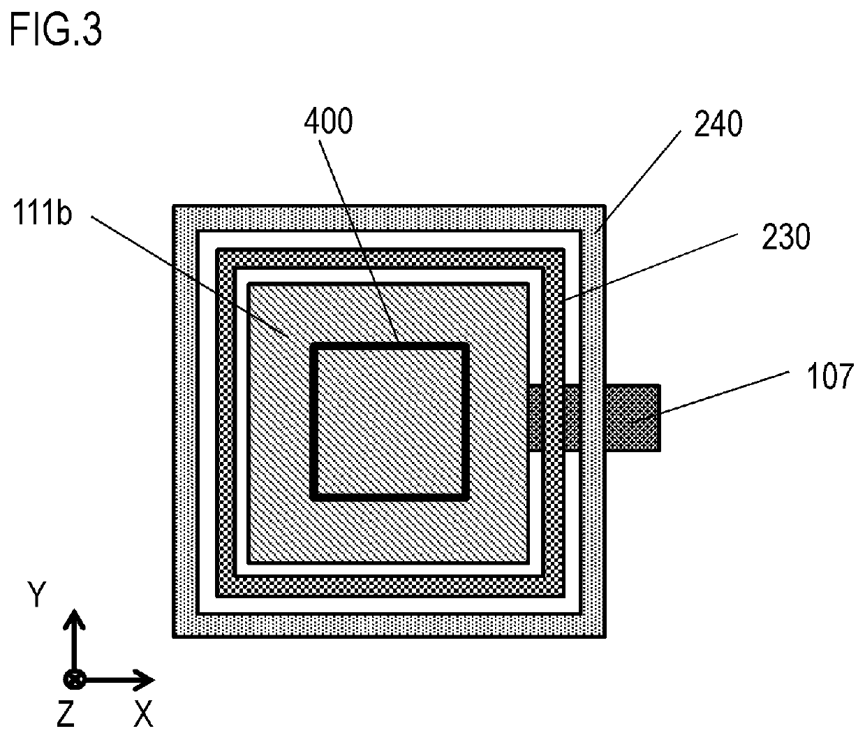
[0146]In the semiconductor device APR according to Modification Example 1, as shown in FIG. 12, a bonding portion 330 located between the conductor portion 113a and the conductor portion 213a is provided in the vicinity of the external connection electrode 111b in the semiconductor device APR. That is, the first semiconductor component 001 and the second semiconductor component 002 in the semiconductor device APR have respective conductor portions 113a and 213a at a distance to the opening 400 which is shorter than the distance between the opening 400 and the guard ring 240 closest to the opening 400. The first semiconductor component 001 and the second semiconductor component 002 are not limited to the case where one conductor portion 113a and one conductor portion 213a satisfying this condition are provided in the respective semiconductor components, and two or more conductor portions may be provided. The distance between the opening 400 and the conductor portions 113a and 213a ma...
modification example 2
[0149]In the semiconductor device APR according to Modification Example 2, as shown in FIG. 14, a guard ring 340 includes the contact plug 204, the wiring layer 205, the via plug 208, the wiring layer 207, the via plug 211, the wiring layer 210, and the bonding region 311. That is, the guard ring 340 has a configuration in which the guard ring 240 in Embodiment 1, the conductor portion 113a and the conductor portion 213a are connected. Further, in the semiconductor device APR according to the present Modification Example, a second guard ring 350 connected on the external connection electrode 111b is formed. The second guard ring 350 is configured to include the connection region 312 and the bonding region 311 in the conductor portion 113a, and the bonding region 321 in the conductor portion 213a. That is, the second guard ring 350 can be formed by bonding the connection region 312 and the bonding region 311 with the bonding region 321, and is configured, for example, of copper as a ...
PUM
 Abstract
Description
Claims
Application Information