Thermoelectric module substrate and thermoelectric module using such board
- Summary
- Abstract
- Description
- Claims
- Application Information
AI Technical Summary
Benefits of technology
Problems solved by technology
Method used
Image
Examples
example 1
1 EXAMPLE 1
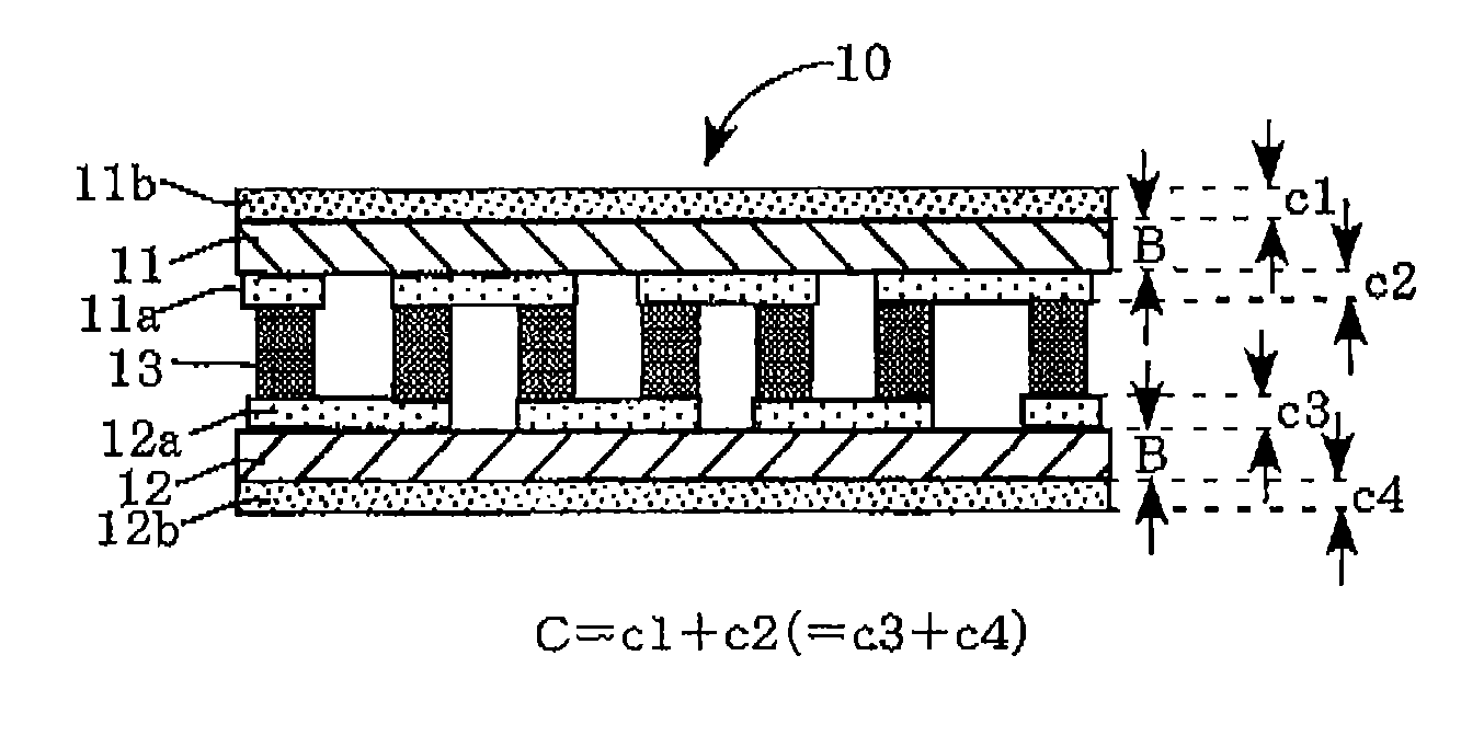
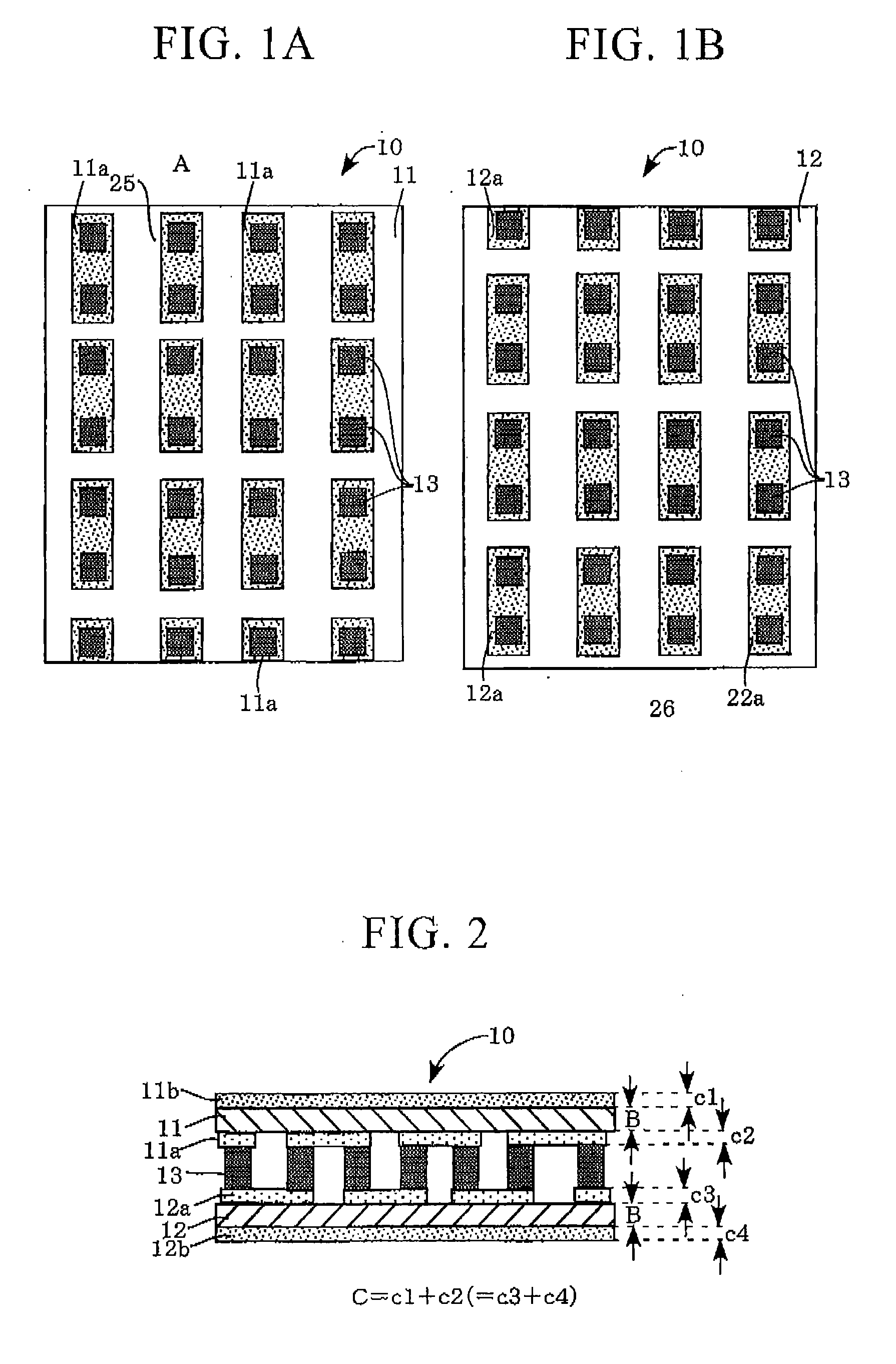
[0025]A synthetic resin layer serving as a thermoelectric module substrate of this example 1 is formed by polyimide resin having electric insulating property, and is formed in a film shape so that thickness (B) of synthetic resin layer falls within a range from 7 μm to 30 μm (7 μm≦B≦30 μm) of the synthetic resin layer, The synthetic resin layer is adapted to constitute an upper substrate 11 as shown in FIG. 1A and a lower substrate 12 as shown in FIG. 1B. In this example, in order to improve thermal conductivity of polyimide resin, fillers at least including alumina powder (average grain diameter is 15 μm or less) are added in a dispersed state. Further, the upper substrate 11 is cut and has a shape in which, for example, the substrate size is 40 mm (width)×40 mm (length). In addition, the lower substrate 12 to which lead wires (not shown) are attached is cut and has a shape in which, for example, the substrate size is 40 mm (width)×45 mm (length).
[0026]In this case, ther...
example 2
2 EXAMPLE 2
[0036]A synthetic resin layer serving as thermoelectric module substrate of this example 2 is caused to be of thermoelectric module configuration similar to the above-described example 1 except that aluminum nitride powders (average grain diameter is 15 μm or less) are dispersed and added as filler, 200 pairs of thermoelectric elements 13 are used with dimensions of 2 mm (length)×2 mm (width)×2 mm (height), an element having composition represented by Bi0.4Sb1.6Te3 is used as P-type semiconductor compound element, an element having composition represented by Bi1.9Sb0.1Te2.7Se0.3 is used as N-type semiconductor element, and shearing extrusion molded body is used.
[0037]Here, in the case where contents volume percentage of fillers existing within synthetic resin layers of upper substrate 11 and lower substrate 12 is expressed as A (vol %), each thickness of the synthetic resin layers of upper substrate 11 and lower substrate 12 is expressed as B (elm), and total thickness of...
example 3
3 EXAMPLE 3
[0044]A synthetic resin layer serving as thermoelectric module substrate of this example 3 is caused to be of the thermoelectric module configuration similar to the above-described example 1 except that epoxy resin is used as resin material, 200 pairs of thermoelectric elements 13 are used with dimensions of 21 mm (length)×2 mm (width)×2 mm (height), an element having composition represented by Bi0.4Sb1.6Te3 is used as P-type semiconductor compound element, an element having composition represented by Bi1.9Sb0.1Te2.7Se0.3 is used as N-type semiconductor compound element, and shearing extrusion molded body is used.
[0045]Here, in the case where contents volume percentage of fillers existing within synthetic resin layers of upper substrate 1 and lower substrate 12 is expressed as A (vol %), each thickness of synthetic resin layers of upper substrate 11 and lower substrate 12 is expressed as B (μm), total thickness of metallic layers at least including wiring pattern (copper ...
PUM
 Abstract
Description
Claims
Application Information

