
Manufacturing optical elements

a technology of optical elements and manufacturing methods, applied in the direction of optics, mountings, lenses, etc., can solve the problems of limited optical design, inability to manufacture lenses on two sides of wafer scale substrates, and inability to meet the so as to reduce the influence of optical properties of optical elements

Active Publication Date: 2011-02-24
AMS SENSORS SINGAPORE PTE LTD
View PDF7 Cites 48 Cited by
  • Summary
  • Abstract
  • Description
  • Claims
  • Application Information

AI Technical Summary

Benefits of technology

[0017]The invention features the important advantage that there are no thickness constraints regarding the design of the optical elements, apart from the requirement that they in themselves have to be mechanically stable (which is not a strong constraint, as the lenses and especially potentially thin sections of them have very small lateral dimensions). In addition, in the case of through holes, the substrate does not need to have optical properties, as no light is passing through it. The substrate becomes uncritical in terms of material and surface quality (scratches etc.) and may. thus, be a lot less costly than prior art substrates. Also in a stack of different wafer-scale assemblies or of different optical elements, space may be saved and potentially the number of components may be reduced, since substrates could be stacked directly on top of each other, or spacers with reduced thickness may be used.
[0031]a contact spacer portion at least partially surrounding or completely surrounding the replication section(s) and being suitable of resting against the substrate surface during replication, so that it forms a seal around the replication section for preventing a lateral (radial) flow of the replication material further than the spacer portion; and of
[0033]In either case, such a replication tool comprising contact spacer portion(s) and / or flow stoppers, is used in combination with dispensing the replication material at the individual replication sites, thus in at least one replication material portion per replication site, where the replication material portions of the different sites stay separate during the whole process. Depending on the application, this may feature substantial advantages over an approach where the replication material is dispensed over a large surface of the substrate. Also, it allows to help the contact spacers to help define the z-dimension of the final, replicated element also in the cases where the replication tool (and / or the substrate) is not dimensionally stiff enough to precisely define said thickness if the relative z-position of the substrate and the replication tool are fixed peripherally.
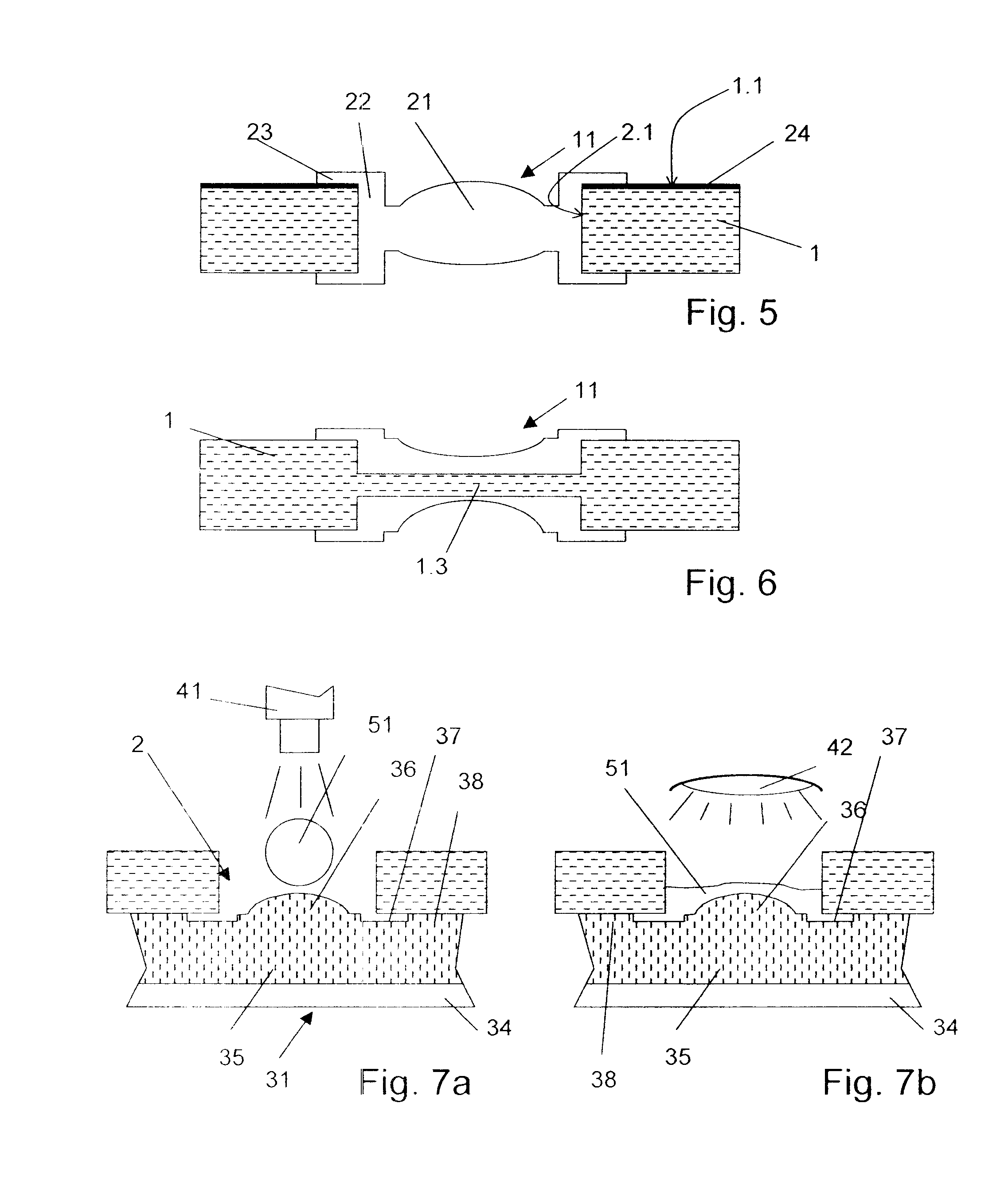
[0035]The contact spacer portions may according to the above, in addition to providing mechanical stability during replication and defining the z-dimension, also have the function of forming a seal preventing lateral flow. This is especially preferred for the and advantageous in the case the replication sites is defined by through holes. Then, preferably the first replication is brought into contact with the substrate from a first side, and the replication material (or a first portion thereof) is dispensed from a second, opposite side into the blind hole that results if the replication tool rests against the substrate and the contact spacer forms a seal somewhere around the first side rim of the through hole.
[0037]In any one of the above-described embodiments, for the mechanical stability of the replicated element and its adhering to the substrate, a replicated base layer may be generated as a part of the replicated optical element structure, the base layer extending outwardly from the edge of the holes and thereby covering a section of the large side of the substrate.

Problems solved by technology

However, the fabrication of a lens on two sides of a wafer scale substrate has some limitations:The substrate thickness needs to have a minimum thickness in order to provide the required mechanical stability, typically of 400μ or greater;For cost reasons, the substrates are often chosen to be off-the-shelf items with a standard thickness.
The range of available standard thicknesses is constrained, and this constriction leads to limitations in the optical design.
According to the depicted state of the art solution, this was not possible.

Method used


Image

  • Manufacturing optical elements
  • Manufacturing optical elements
  • Manufacturing optical elements

Examples


Embodiment Construction

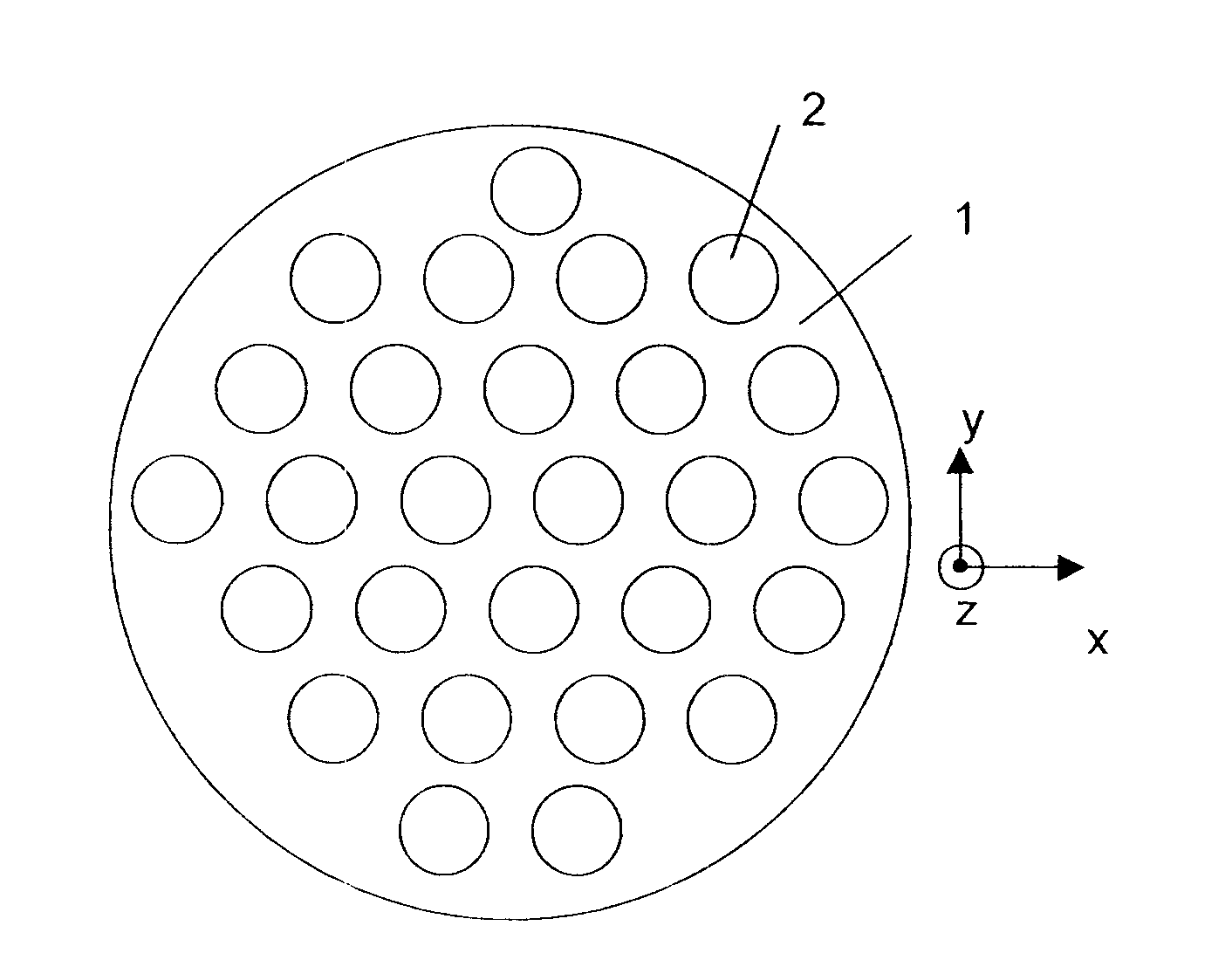
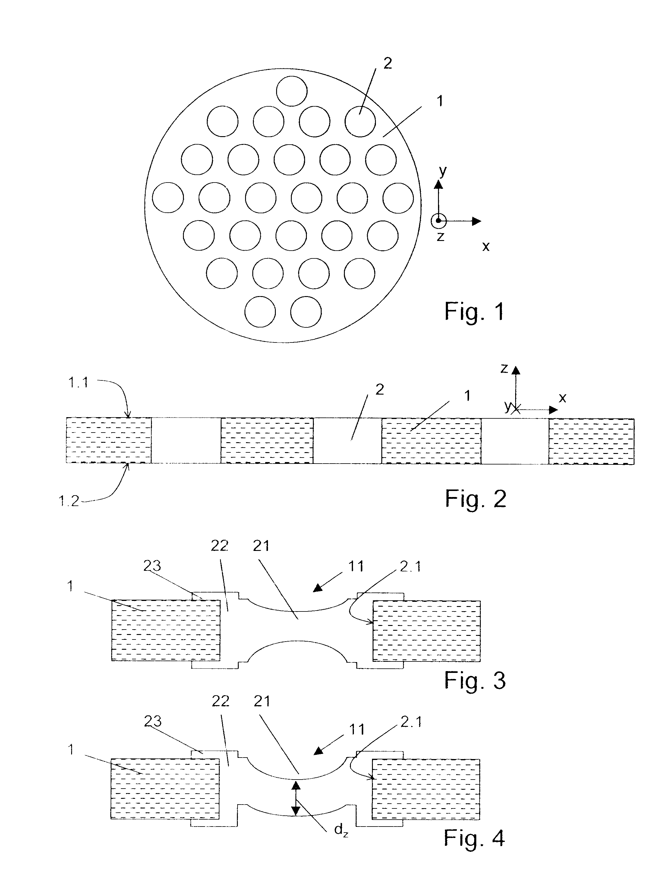
[0055]The substrate 1 schematically depicted in FIG. 1 is essentially flat with a plurality of replication sites defined by holes 2 in the substrate. Preferably, the substrate is wafer-scale. The arrangement of the holes on a large surface may be in a regular pattern to ease subsequent process steps such as dicing (dividing the optical assembly after replication, and potentially after further method steps such as stacking with other wafer-scale elements, into the individual elements).

[0056]The substrate used for the different embodiments of the invention may be transparent. It may be made of glass or of an organic or inorganic plastic material or of any suitable transparent material providing sufficient dimensional stiffness.

[0057]The substrate, according to an alternative, may be nontransparent. Especially, the substrate, if the replication sites are defined by through holes, may even be nontransparent in case the manufactured optical elements are lenses. A nontransparent substrate...


PUM


Abstract

A method of replicating at least one optical element is provided, the method including the steps of: providing a substrate with two large sides and at least one pre-defined replication site defined by a through hole or blind holes at corresponding locations on both large sides of the substrate; and adding, by replication, a replicated structure to the substrate, the replicated structure adhering to the substrate and having, at the replication site, replication material in the through hole or in the two blind holes, respectively and a first replicated surface and a second replicated surface, the first and second replication surfaces facing towards opposite sides.

Description

BACKGROUND OF THE INVENTION[0001]1. Field of the Invention[0002]The invention is in the field of manufacturing a plurality of optical elements, for example refractive optical lenses or diffractive micro-optical lenses, preferably on a waver scale by means of a replication process that includes embossing steps. More concretely, it deals with a method of replicating a plurality of optical elements.[0003]2. Description of Related Art[0004]Replicated optical elements include transparent diffractive and / or refractive optical elements for influencing an optical beam in any pre-defined manner, refractive elements such as lenses, potentially at least partially reflecting elements etc..[0005]When optical elements are produced by replication, there is often a basic configuration involving a substrate and a replication tool, and replication material being placed in contact with the substrate and / or the replication tool. The replication tool comprises a replication structure being the negative ...

Claims


Application Information

Patent Timeline
IPC IPC(8): G02B3/00B29D11/00
CPCB29D11/00375
Inventor ROSSI, MARKUSRUDMANN, HARTMUT
Owner AMS SENSORS SINGAPORE PTE LTD
Learn More