Advanced Modulation Formats for Silicon-Based Optical Modulators

a technology of optical modulators and modulators, applied in the direction of optical elements, optical waveguide light guides, instruments, etc., can solve the problems of inability to use lithium niobate-based optical devices in such a situation, inability to achieve data rate data rates, and inability to meet the requirements of relatively complex electrical drive structures

Active Publication Date: 2011-02-24
CISCO TECH INC
View PDF9 Cites 70 Cited by
  • Summary
  • Abstract
  • Description
  • Claims
  • Application Information

AI Technical Summary

Benefits of technology

[0017]Advantageously, the inclusion of multiple modulator segments controlled by an encoding of the digital input signal allows for

Problems solved by technology

Clearly, the use of lithium niobate-based optical devices in such a situation is not an option.
Moreover, it is well-known that any of these field-based devices have inherent performance limitations at data rates exceeding, for examp

Method used


Image

  • Advanced Modulation Formats for Silicon-Based Optical Modulators
  • Advanced Modulation Formats for Silicon-Based Optical Modulators
  • Advanced Modulation Formats for Silicon-Based Optical Modulators

Examples


Embodiment Construction

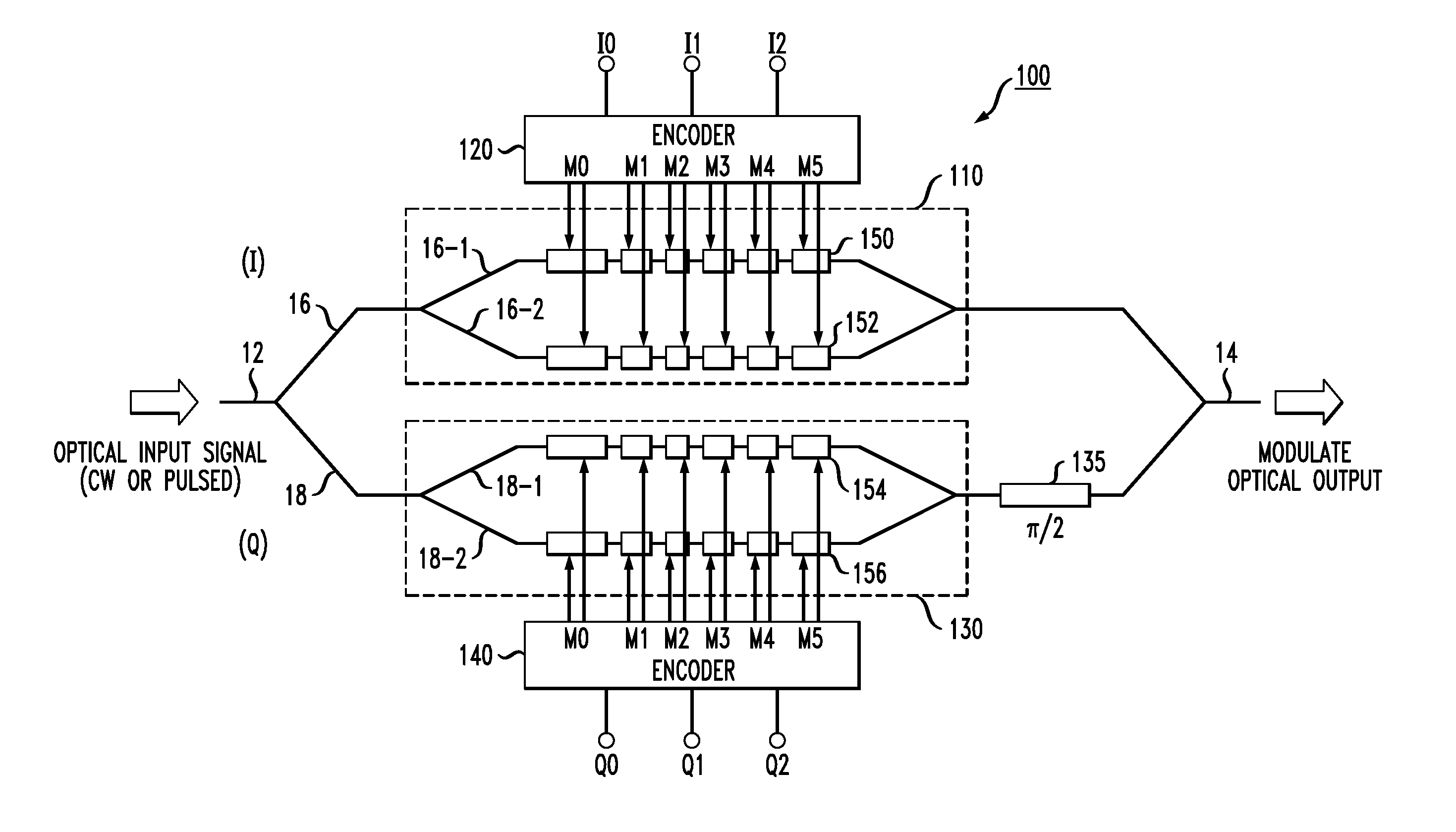
[0035]FIG. 7 illustrates an exemplary silicon-based optical modulator 30 formed in accordance with the present invention to address the nonlinearity and attenuation problems associated with the use of free carrier dispersion-based modulation in a multi-segment modulator configuration. As shown, modulator 30 comprises the same MZI architecture as discussed above, including an input waveguide 12, output waveguide 14 and a pair of waveguiding arms 16, 18. A CW optical signal is coupled into input waveguide 12 and a “modulated” optical signal appears along output waveguide 14, the modulation introduced by an electrical input (data) signal applied as an input to modulating devices disposed along waveguide arms 16, 18. Each waveguide arm 16, 18 is shown as comprising multiple segments, with the electrical (data) input signals used to control the degree of phase modulation introduced into the propagating optical signal.

[0036]In particular, optical waveguide arm 16 is shown as comprising a ...


PUM


Abstract

A silicon-based optical modulator is configured as a multi-segment device that utilizes a modified electrical data input signal format to address phase modulation nonlinearity and attenuation problems associated with free-carrier dispersion-based modulation. The modulator is formed to include M separate segments and a digital signal encoder is utilized to convert an N bit input data signal into a plurality of M drive signals for the M modulator segments, where M≧2N/2. The lengths of the modulator segments may also be adjusted to address the nonlinearity and attenuation problems. Additional phase adjustments may be utilized at the output of the modulator (beyond the combining waveguide).

Description

CROSS-REFERENCE TO RELATED APPLICATIONS[0001]This application claims the benefit of U.S. Provisional Application No. 61 / 235,106 filed Aug. 19, 2009 and U.S. Provisional Application No. 61 / 355,374, filed Jun. 16, 2010, both of which are herein incorporated by reference.TECHNICAL FIELD[0002]The present invention relates to silicon-based optical modulators and, more particularly, to a segmented silicon-based optical modulator utilizing a digital encoder for mapping a multi-bit input data signal into a plurality of signals for driving the separate modulator segments in a combination that is selected to address performance problems (e.g., attenuation) associated with unique properties of silicon-based modulators.BACKGROUND OF THE INVENTION[0003]For many years, optical modulators have been made out of electro-optic material, such as lithium niobate. Optical waveguides are formed within the electro-optic material, with metal contact regions disposed on the surface of each waveguide arm. A ...

Claims


Application Information

Patent Timeline
IPC IPC(8): G02F1/035
CPCG02F1/0121G02F1/2257G02F2001/0152H04B10/516H04B10/5053H04B10/5055H04B10/5051G02F1/0152
Inventor WEBSTER, MARKSHASTRI, ANUJITSHASTRI, KALPENDU
Owner CISCO TECH INC
Why Eureka
Try Eureka