Electrophoretic display panel

a display panel and electrophoretic technology, applied in the field of electrophoretic display panels, can solve the problems of difficult arrangement of electrodes and interconnection lines

Inactive Publication Date: 2011-03-10
CASIO COMPUTER CO LTD
View PDF8 Cites 18 Cited by
  • Summary
  • Abstract
  • Description
  • Claims
  • Application Information

AI Technical Summary

Benefits of technology

[0010]Additional objects and advantages of the invention will be set forth in the description which follows, and in part will be obvious from the description, or may be learned by practice of the invention. The objects and advantages of the invention may be realized and obtained by means of the instrumentalities and combinations particularly pointed out hereinafter.

Problems solved by technology

For this reason, when a high-resolution electrophoretic display panel including a lot of pixels is needed, it is difficult to arrange the electrodes and the interconnection lines.

Method used


Image

  • Electrophoretic display panel
  • Electrophoretic display panel
  • Electrophoretic display panel

Examples


first embodiment

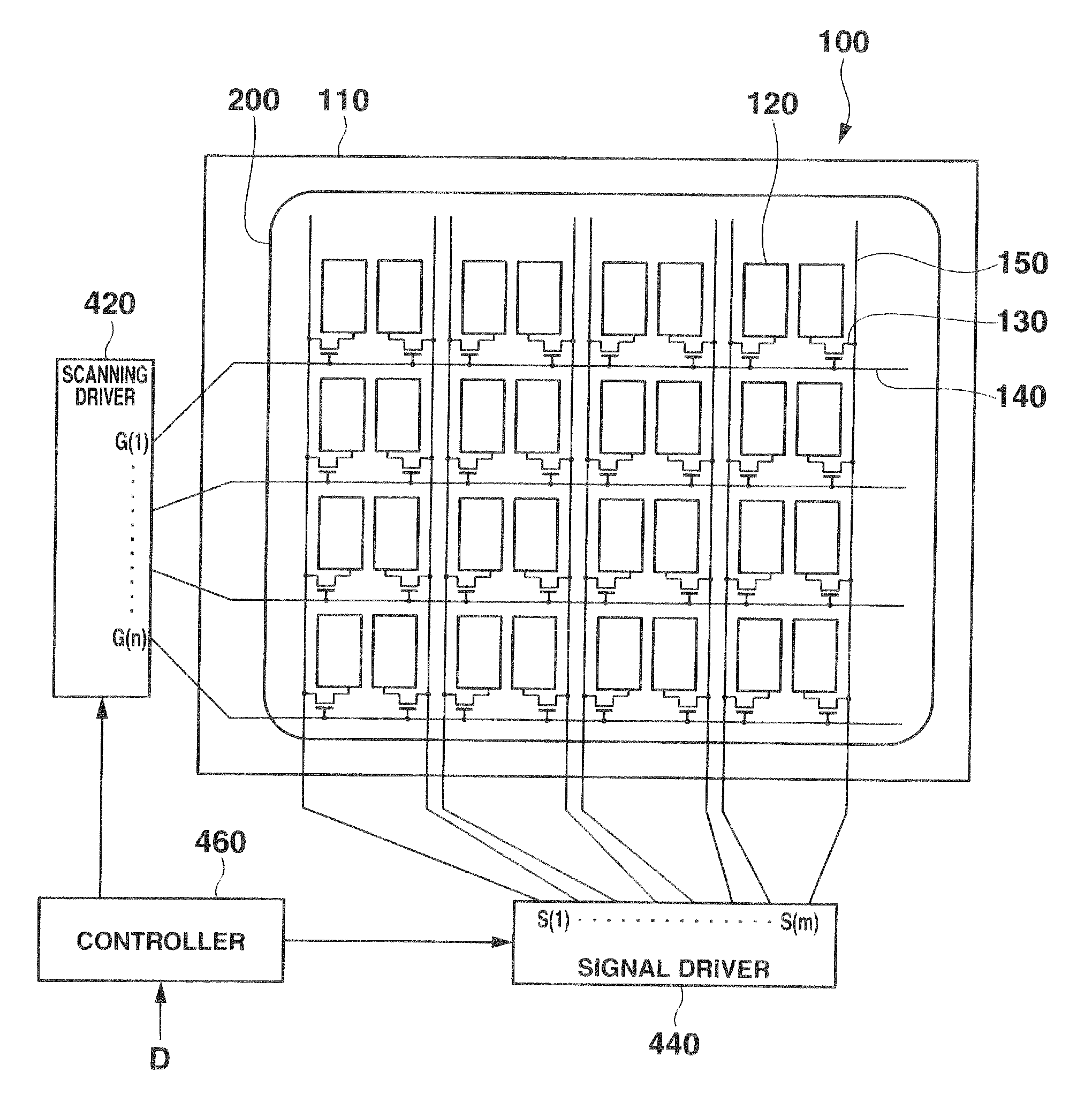
[0027]The first embodiment of the present invention will be described first with reference to the accompanying figures. FIG. 1 is a view showing the arrangement of a display apparatus including an electrophoretic display panel according to the embodiment. As shown in FIG. 1, the electrophoretic display apparatus includes a display panel 100, a scanning driver 420, a signal driver 440, and a controller 460. The display panel 100 displays an image based on image data D supplied out of the electrophoretic display apparatus. The display panel 100 includes a display device having an electrophoretic layer sandwiched between a pixel-side substrate 110 and a COM substrate 200.

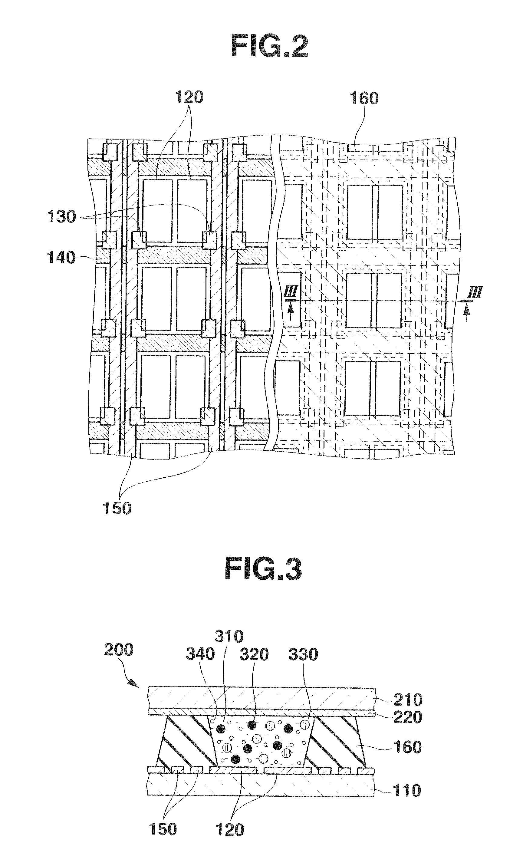
[0028]A plurality scanning lines 140 (G(j) (j=1, 2, . . . , n)) and a plurality of signal lines 150 (S(i) (i=1, 2, . . . , m)) run so as to intersect each other on the pixel-side substrate 110. A pixel electrode 120 is arranged at each of positions corresponding to the intersections between the scanning lines 140 and t...

second embodiment

[0048]The second embodiment of the present invention will be described low with reference to the accompanying figures. Only the differences from the first embodiment will be described here. In the first embodiment, the pixel electrode 120 has a rectangular shape with one corner cut away, and two pixel electrodes are arranged per pixel to be line-symmetrical, as shown in FIG. 10. In the first embodiment, when one pixel electrode 120 in one pixel is set at a positive voltage, and the other pixel electrode 120 is set at a negative voltage for white display, the positively-charged black particles 320 and the negatively-charged red particles 330 gather on the negative electrode and the positive electrode, respectively. When the shield of the neutral white particles 340 is sufficient, the observer cannot view the state in which the positively-charged black particles 320 and the negatively-charged red particles 330 gather on the corresponding electrodes and are thus separated into two. Con...

third embodiment

[0052]The third embodiment of the present Invention will be described below with reference to the accompanying figures. Only the differences from the first and second embodiments will be described here as well. In the first and second embodiments, the adjacent and opposite sides of the two pixel electrodes 120 in one pixel are linear. The scanning lines, signal line, and capacity lines are linear, too. For this reason, when the shield of the neutral white particles 340 is insufficient, the adjacent and opposite sides of the two pixel electrodes 120 in one pixel may interfere with the scanning lines, the signal line, and the capacity lines. As a result, interference fringes will be generated. The interference fringes may generate noise that deteriorates the display quality of the electrophoretic display panel. To prevent this, in the third embodiment, the adjacent and opposite sides of two pixel electrodes 120 in one pixel are curved.

[0053]FIG. 14 shows an example of the shape of the...


PUM

PropertyMeasurementUnit
linear shapeaaaaaaaaaa
curved shapeaaaaaaaaaa
areasaaaaaaaaaa

Abstract

An electrophoretic display panel includes a first substrate, a second substrate, a partition wall, first electrodes, a second electrode, a dispersant, positively-charged particles, negatively-charged particles, weakly-charged particles, switching thin film transistors, scanning lines, and signal lines. Pixel spaces are surrounded by the partition wall, the first substrate and the second substrate. Two of the first electrodes are formed on the first substrate in each pixel. The second electrode facing the first electrodes is formed on the second substrate. The dispersant with the positively-charged particles, the negatively-charged particles, and weakly-charged particles is contained in the pixel spaces. The switching thin film transistors are connected to the first electrode, and the signal line. The scanning lines supply scanning signals to gate electrodes of the switching thin film transistors. The signal lines input a data signal to the switching thin film transistors.

Description

CROSS-REFERENCE TO RELATED APPLICATIONS[0001]This application is based upon and claims the benefit of priority from the prior Japanese Patent Application No. 2009-206289, filed. Sep. 7, 2009, the entire contents of which are incorporated herein by reference.BACKGROUND OF THE INVENTION[0002]1. Field of the Invention[0003]The present invention relates to an electrophoretic display panel.[0004]2. Description of the Related Art[0005]An electrophoretic display device is beginning to find application in such fields as electronic book readers, cellular phones, electronic shelf labels, and watches. The electrophoretic display device is capable of display easy on eyes because it can obtain a reflectivity, contrast, and angle of view close to those of paper. Since the electrophoretic display device has a memory property, the device consumes power only for display rewrite, and requires no more power once data is displayed. That is, the electrophoretic display device is a low power consumption ...

Claims


Application Information

Patent Timeline
Patent Type & Authority Applications(United States)
IPC IPC(8): G09G3/34G02F1/167G02F1/16762G02F1/16766
CPCG02F1/167G02F2001/1676G09G2300/0842G09G3/3446G09G3/2003G02F1/16762G02F1/16766G02F1/1681G02F2001/1678G02F2201/123G02F2201/121
Inventor MIYASHITA, TAKASHI
Owner CASIO COMPUTER CO LTD
Why Eureka
Try Eureka