Dry film and manufacturing method of dry film
- Summary
- Abstract
- Description
- Claims
- Application Information
AI Technical Summary
Benefits of technology
Problems solved by technology
Method used
Image

Examples
first embodiment
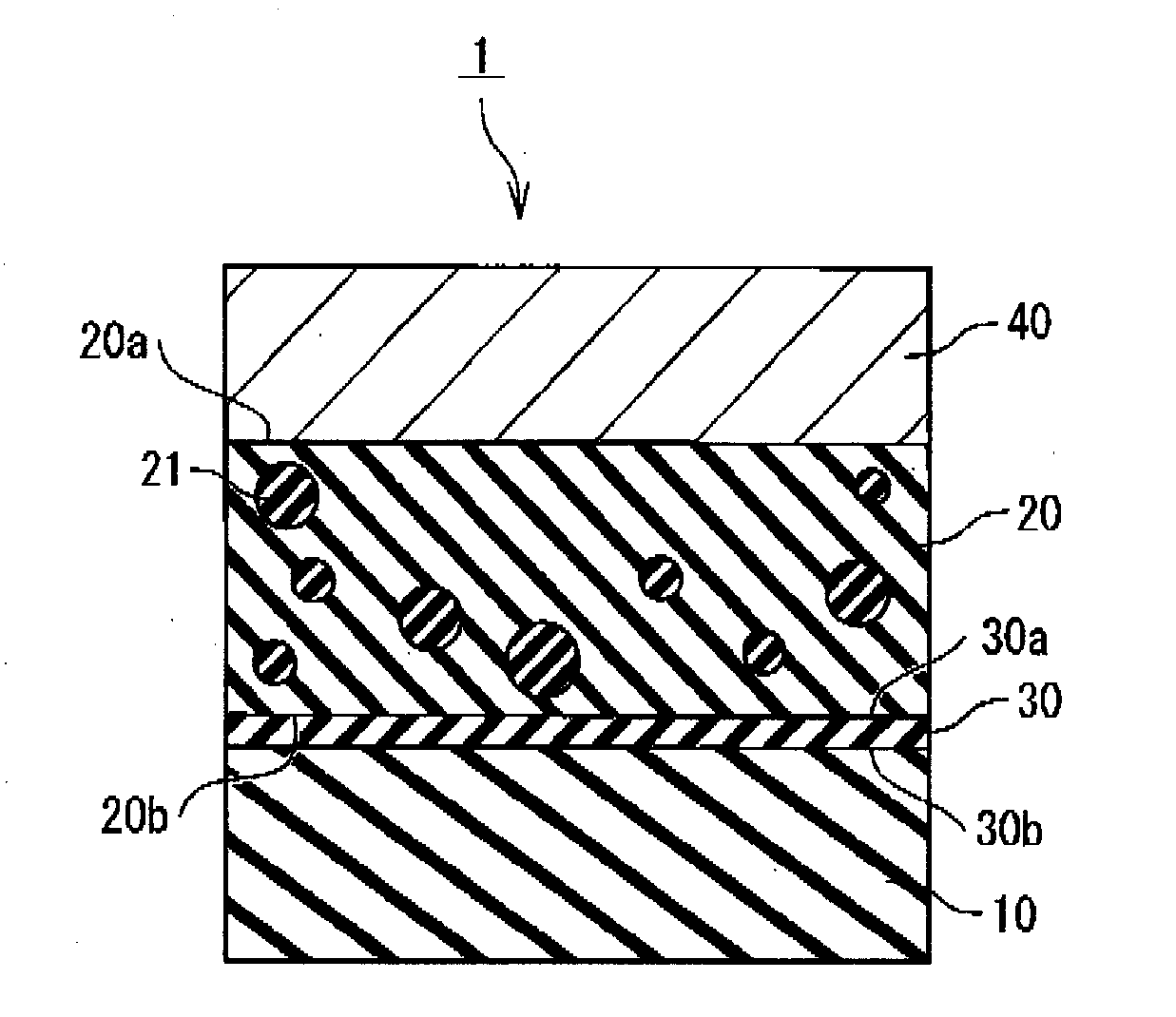
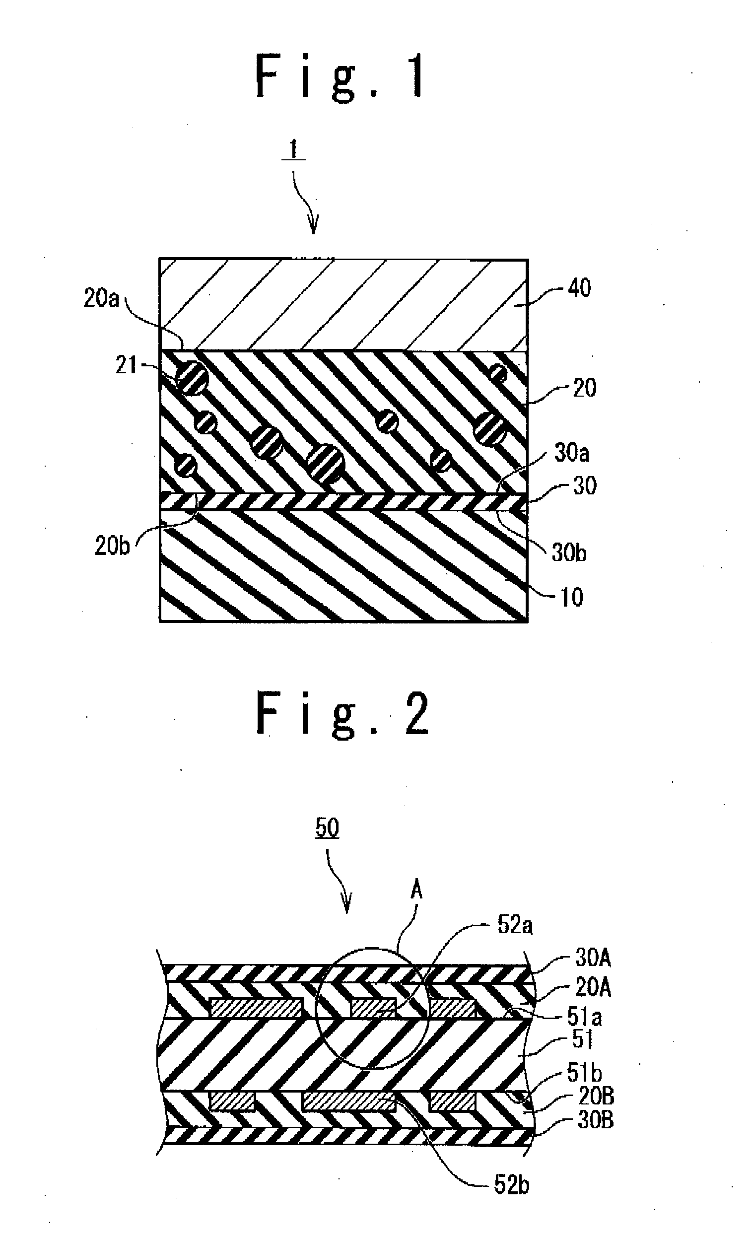
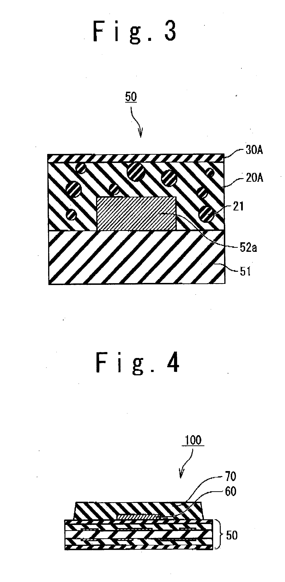
[0032]A first embodiment of the present invention is described below. FIG. 1 is a sectional view of a dry film 1 according to the present embodiment. Referring to FIG. 1, the dry film 1 includes a supporting film 10, a solder resist film 20, a second solder resist film 30 and a protection film 40.
[0033]The supporting film 10 is a base material on which the solder resist film 20, the solder resist film 30 and the protection film 40 are formed. The supporting film 10 prevents deformations of the solder resist film 20, the solder resist film 30 and the protection film 40. A known material which can support the solder resist film can be used to form the supporting film 10. For example, in addition to polyester such as PET (polyethylene terephthalate) and PEN (polyethylene naphthalate), polypropylene and polyethylene can be used.
[0034]The solder resist film 20 and the solder resist film 30 are insulating films formed on the supporting film 10. Specifically, the solder resist film 30 is f...
second embodiment
[0067]A second embodiment of the present invention is described. A dry film 1 according to the second embodiment of the present invention is different from the dry film 1 according to the first embodiment in the configuration of the solder resist film 30. Since the other configurations are the same as those of the first embodiment, the same components are denoted by the same reference symbols and the explanations thereof are omitted. FIG. 9 is a partial sectional view showing the dry film 1 according to the second embodiment of the present invention.
[0068]Referring to FIG. 9, the dry film 1 includes the supporting film 10, the solder resist film 20, a solder resist film 35 and the protection film 40. The supporting film 10, the solder resist film 20 and the protection film 40 are the same as those of the first embodiment.
[0069]The solder resist film 35 includes second elastomer 36. Similarly to the first elastomer 21, the second elastomer 36 is polymer dispersed as particles in the ...
third embodiment
[0077]A third embodiment of the present invention is described. The third embodiment is a combination of the first embodiment and the second embodiment. Therefore, components same as those of the first and second embodiments are denoted by the same reference symbols and the explanations thereof are omitted.
[0078]FIG. 12 is a sectional view of the dry film 1 according to the third embodiment of the present invention. Referring to FIG. 12, the dry film 1 according to the third embodiment of the present invention includes the supporting film 10, the solder resist film 20, the solder resist film 35, a solder resist film 37 and the protection film 40. The supporting film 10, the solder resist film 20, the solder resist film 35 and the protection film 40 are the same as those of the first or second embodiments.
[0079]Referring to FIG. 12, the solder resist film 37 is described. The solder resist film 37 is formed between the supporting film 10 and the solder resist film 35. Therefore, when...
PUM
| Property | Measurement | Unit |
|---|---|---|
| Thickness | aaaaa | aaaaa |
| Diameter | aaaaa | aaaaa |
| Adhesion strength | aaaaa | aaaaa |
Abstract
Description
Claims
Application Information
 - R&D Engineer
- R&D Manager
- IP Professional
- Industry Leading Data Capabilities
- Powerful AI technology
- Patent DNA Extraction
Browse by: Latest US Patents, China's latest patents, Technical Efficacy Thesaurus, Application Domain, Technology Topic.
© 2024 PatSnap. All rights reserved.Legal|Privacy policy|Modern Slavery Act Transparency Statement|Sitemap