Semiconductor processing apparatus with simultaneously movable stages

a technology of semiconductor wafers and processing equipment, applied in the direction of photomechanical equipment, instruments, printers, etc., can solve the problems of inaccurate readings, affecting the positioning of semiconductors, and poor resolution of features formed on semiconductor wafers

Active Publication Date: 2011-04-14
TAIWAN SEMICON MFG CO LTD
View PDF3 Cites 320 Cited by
  • Summary
  • Abstract
  • Description
  • Claims
  • Application Information

AI Technical Summary

Problems solved by technology

The disturbances and vibrations produced as stage 3 moves along direction 11 adversely affect the positioning of semiconductor wafer 17 and produce various problems such as misalignment, inaccurate readings, and poor resolution of features formed on semiconductor wafer 17 such as due to poor or varying focus.
Conventional tools and methods therefore suffer the shortcomings of vibrations or other disturbances in the motion of the stage, the requirement to use a massive mass balance to counteract the motion of the stage, or both.

Method used


Image

  • Semiconductor processing apparatus with simultaneously movable stages
  • Semiconductor processing apparatus with simultaneously movable stages
  • Semiconductor processing apparatus with simultaneously movable stages

Examples


Embodiment Construction

[0016]The invention provides a system and method for manufacturing semiconductor devices. The system and method involve simultaneously processing two or four or other numbers of semiconductor wafers in a processing operation and in a processing apparatus that involves movement of the wafers. In one exemplary embodiment, an apparatus includes two semiconductor wafers disposed on chucks and parallel and co-planar with one another wherein the wafers undergo processing while moving in opposite directions. In another exemplary embodiment, four wafers are processed simultaneously and each pair of two wafers includes the wafers moving in opposite directions while a processing operation is being performed upon the wafers.

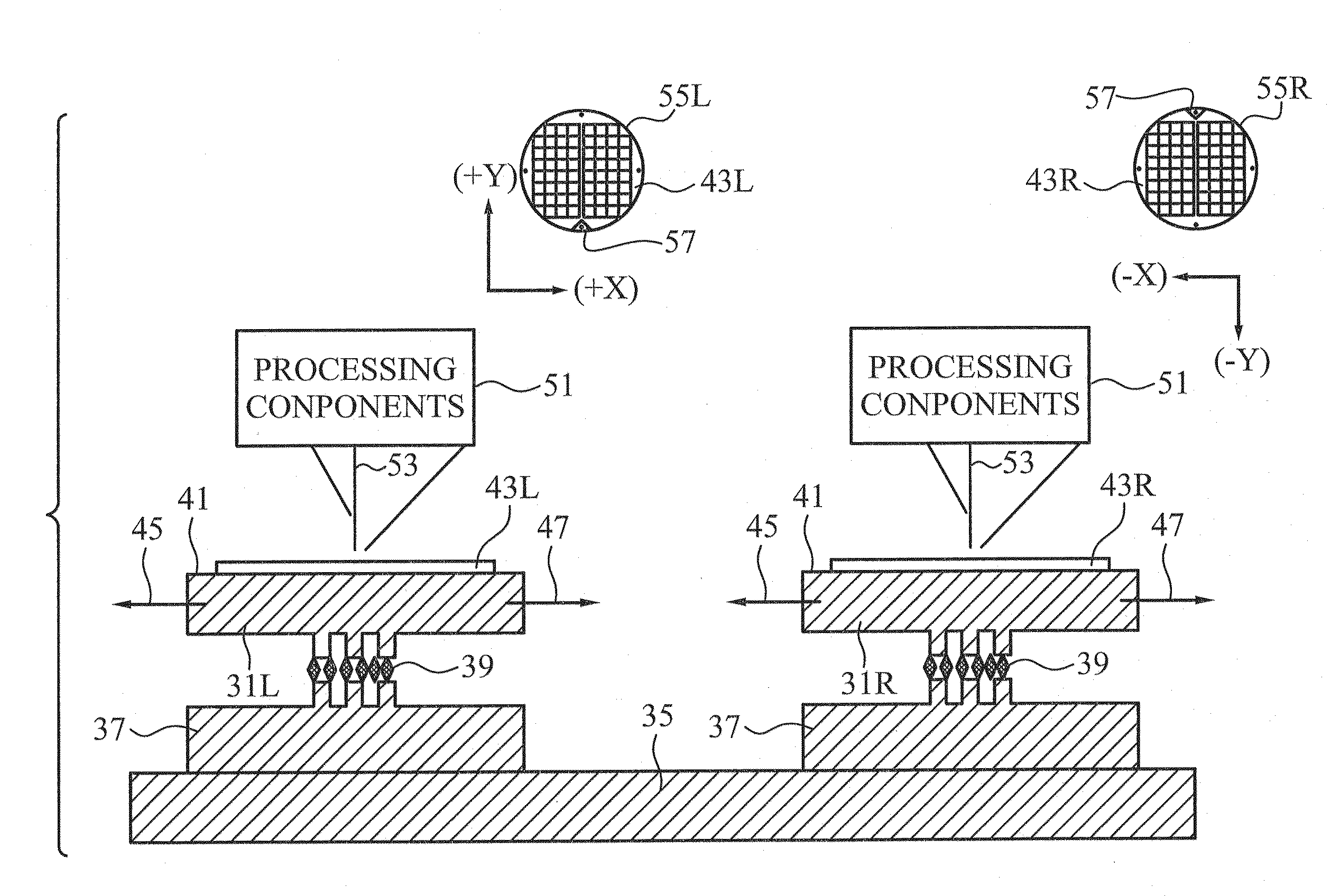
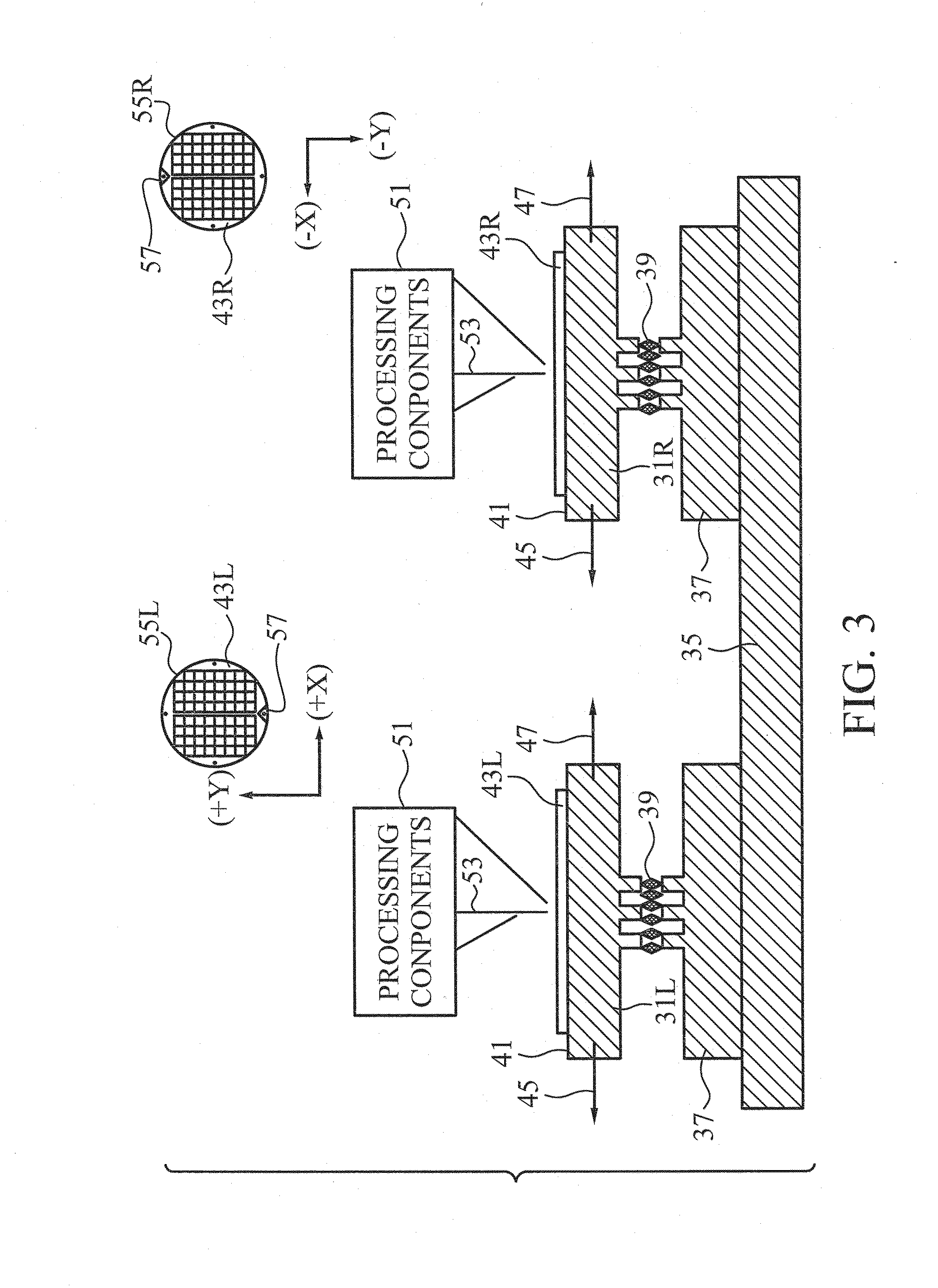
[0017]FIG. 3 shows an exemplary apparatus according to the invention. FIG. 3 shows left stage 31L and right stage 31R disposed over fixed base 35 of a semiconductor manufacturing apparatus. Fixedly coupled to fixed base 35 is hardware 37. The semiconductor processing appara...


PUM

PropertyMeasurementUnit
weight ratioaaaaaaaaaa
diametersaaaaaaaaaa
diameteraaaaaaaaaa

Abstract

A method and apparatus provide for simultaneously moving multiple semiconductor wafers in opposite directions while simultaneously performing processing operations on each of the wafers. The semiconductor wafers are orientated in coplanar fashion and are disposed on stages that simultaneously translate in opposite directions to produce a net system momentum of zero. The die of the respective semiconductor wafers are processed in the same spatial sequence with respect to a global alignment feature of the semiconductor wafer. A balance mass is not needed to counteract the motion of a stage because the opposite motions of the respective stages cancel each other.

Description

FIELD OF THE INVENTION[0001]The invention relates to semiconductor manufacturing equipment and, more particularly, to semiconductor manufacturing tools that simultaneously process multiple wafers at the same time using process operations that involve movement of semiconductor wafers during processing.BACKGROUND[0002]In today's advancing semiconductor manufacturing industry, increased integration levels and decreased feature sizes mandate the use of highly accurate and precise semiconductor manufacturing equipment. When the manufacturing tool involves the movement of the semiconductor wafer before or during processing, the movement must be highly precise and accurate and free from vibration or other disturbances that can displace the semiconductor wafer and result in misalignment, poor feature resolution, or other anomalies or defects.[0003]It is also of critical importance to manufacture as many semiconductor devices as possible within a given time period and similarly important to ...

Claims


Application Information

Patent Timeline
Patent Type & Authority Applications(United States)
IPC IPC(8): G01N33/00G01N21/55G03B27/52
CPCB82Y10/00B82Y40/00G03F7/70525G03F7/70725H01L21/68785G03F7/70766H01J37/3174H01L21/68G03F7/70733
Inventor LIN, YU-FUCHEN, YUNG-CHENGLEE, HENG-JENLIN, CHIN-HSIANG
Owner TAIWAN SEMICON MFG CO LTD
Why Eureka
Try Eureka