

Chip package and fabrication method thereof
- Summary
- Abstract
- Description
- Claims
- Application Information
AI Technical Summary
Problems solved by technology
Method used
Image

Examples
Embodiment Construction
[0017]The following description is of the fabrication and the use of carrying out the invention. It can be understood that this description is provided for the purpose of illustrating the fabrication and the use of the invention and should not be taken in a limiting sense.
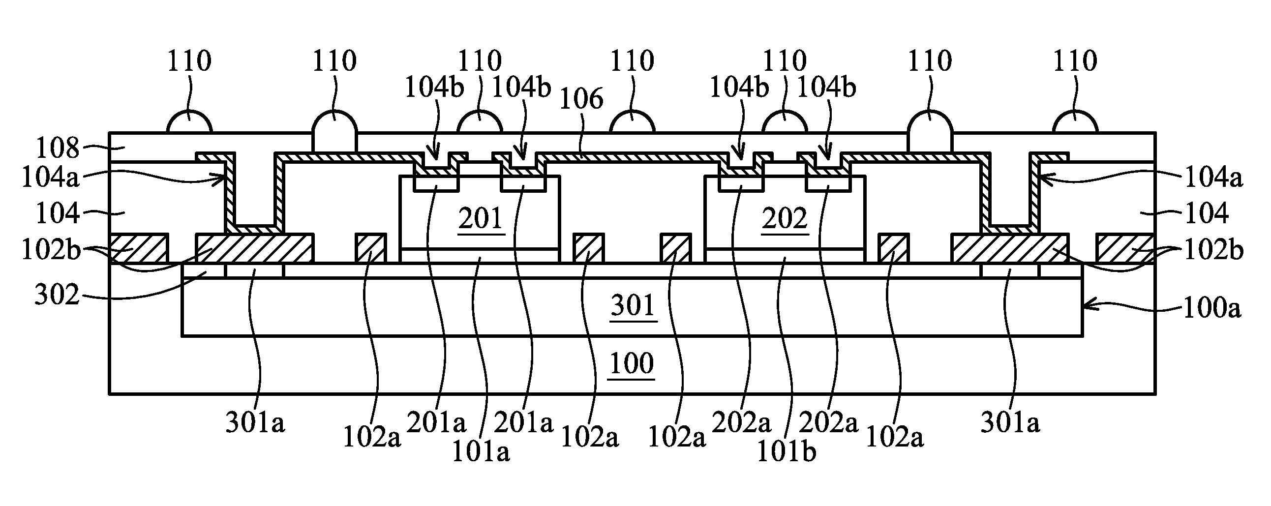
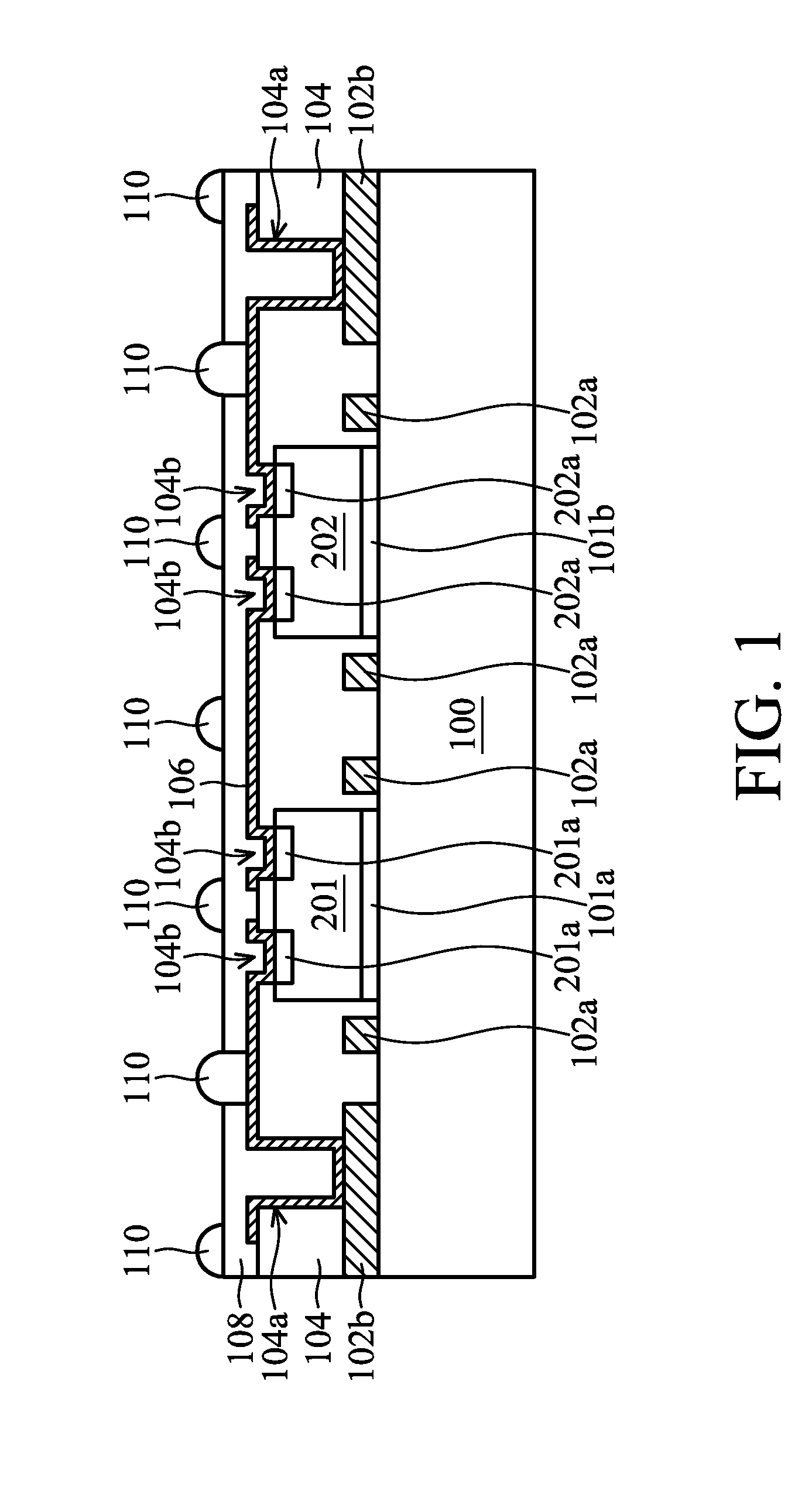
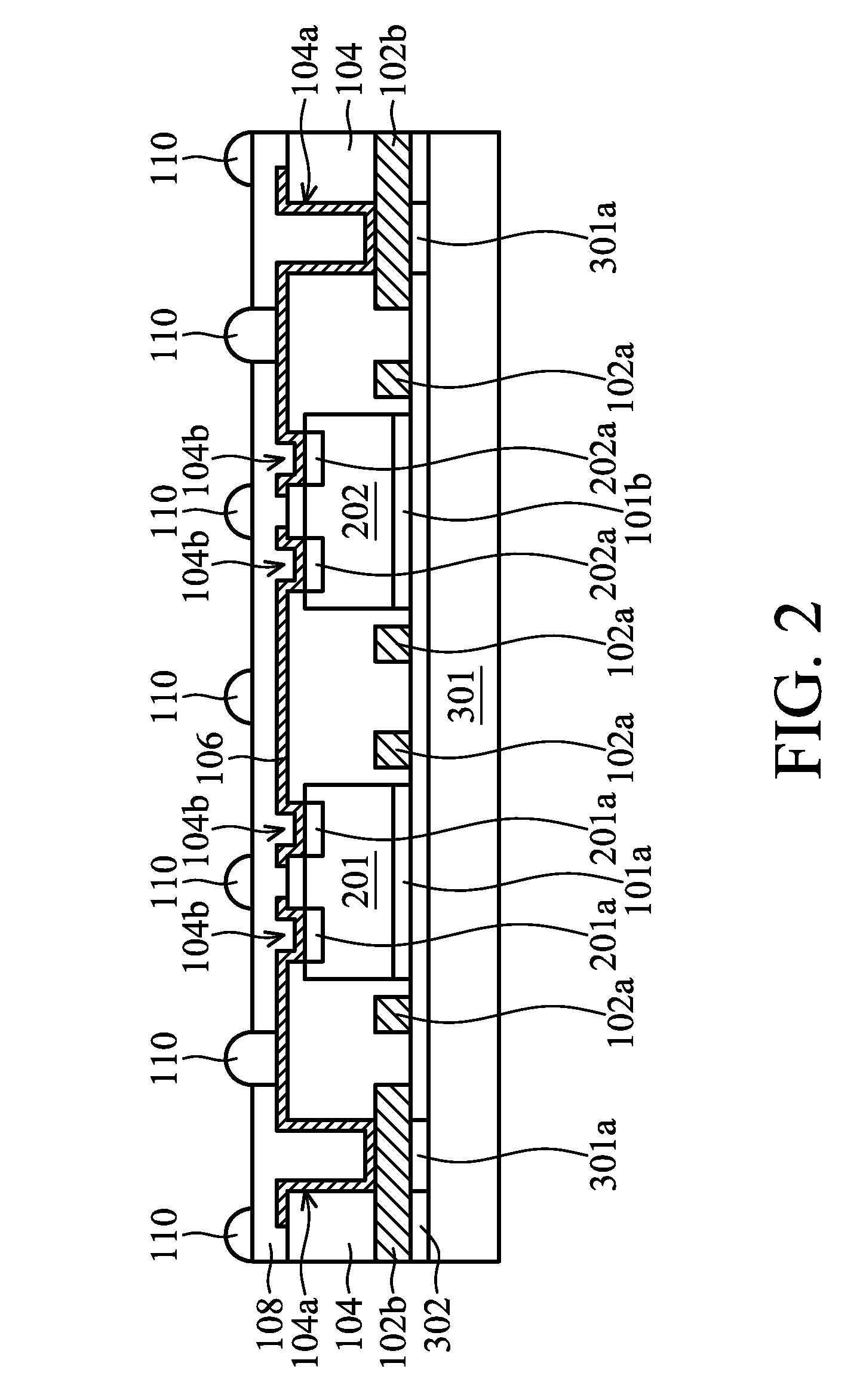
[0018]Referring to FIGS. 1 to 3, which are cross sections of various exemplary embodiments of a chip package according to the invention. In the embodiments, the chip package may be applied in various electronic components including active or passive elements, digital or analog integrated circuits, such as optoelectronic devices, micro electro mechanical systems (MEMS), micro fluidic systems, and physical sensors for detecting physical characteristics such as detecting heat, light, or pressure. In particular, a wafer level package (WLP) process may be performed to package semiconductor chips which include image sensor devices, light-emitting diodes (LEDs), solar cells, RF circuits, accelerators, gyroscopes, micro ac...
PUM
 Abstract
Description
Claims
Application Information