

Display device
a display device and display technology, applied in the field of display devices, can solve the problems of increasing the overall thickness of the display device, reducing the display quality, and increasing the weigh
- Summary
- Abstract
- Description
- Claims
- Application Information
AI Technical Summary
Benefits of technology
Problems solved by technology
Method used
Image

Examples
first embodiment
Advantages of First Embodiment
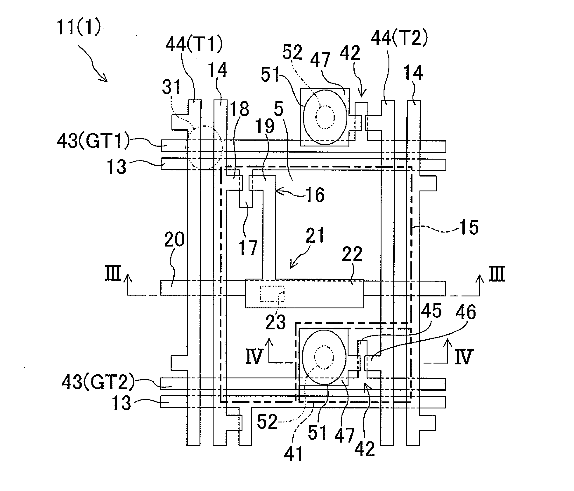
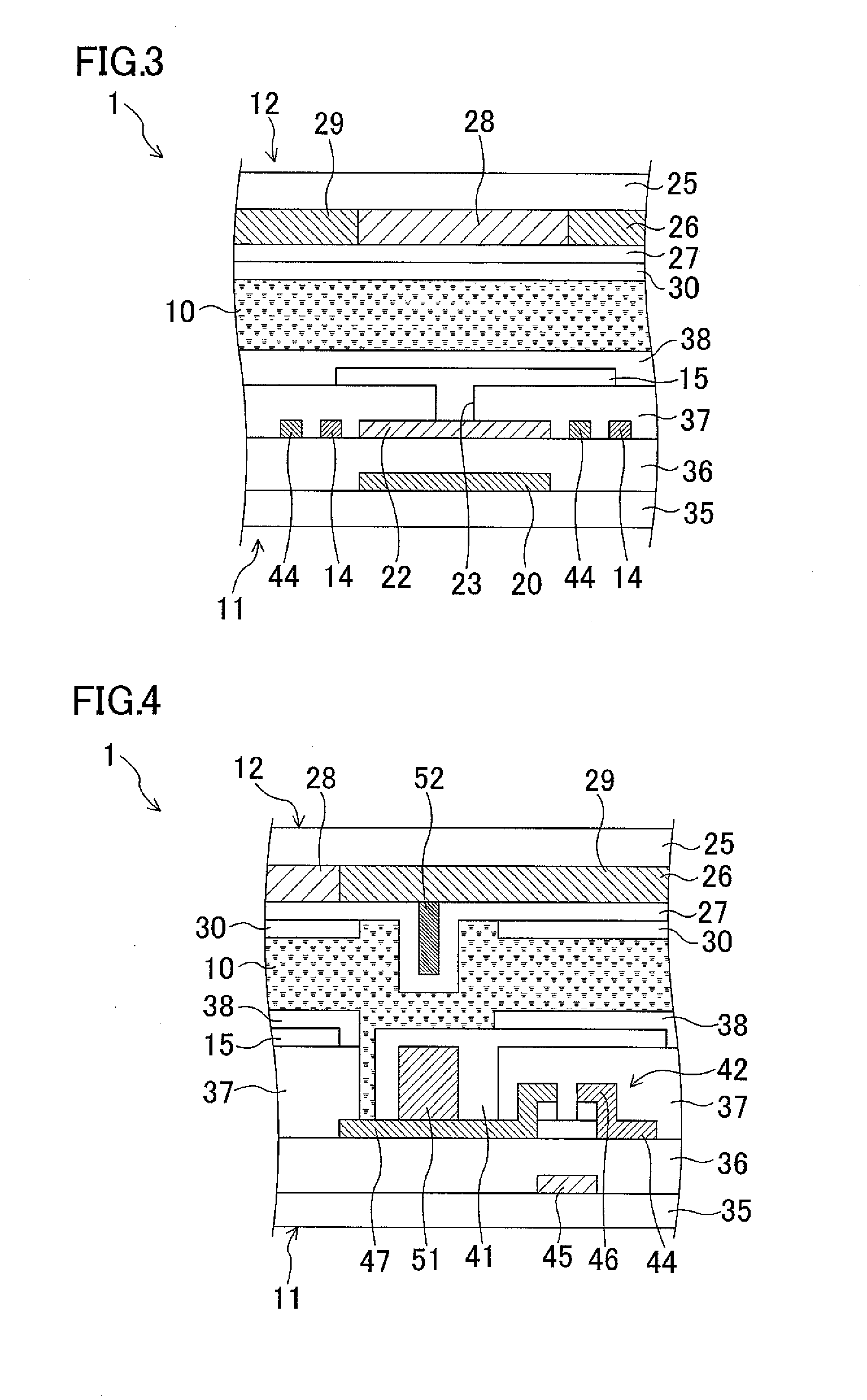
[0092]Thus, according to the first embodiment, the touch electrode 41, which contacts the counter electrode 27 when the counter substrate 12 is pressed, and the detection element 42 for detecting electrical connection between the touch electrode 41 and the counter electrode 27 are provided in each pixel 5. This enables the configuration with a small overall thickness to be implemented, and enables the touched positions of multiple points to be simultaneously detected.
[0093]Moreover, since a plurality of optical sensors are not provided, the touched position can be accurately detected with a simple configuration, regardless of the brightness of ambient light. In addition, the device cost can be reduced, and a decrease in aperture ratio can reduced, whereby the display quality can be increased.
[0094]Furthermore, since the first protruding portion 51 is provided in the TFT substrate 11, and the second protruding portion 52 is provided in the counter substr...
second embodiment
Advantages of Second Embodiment
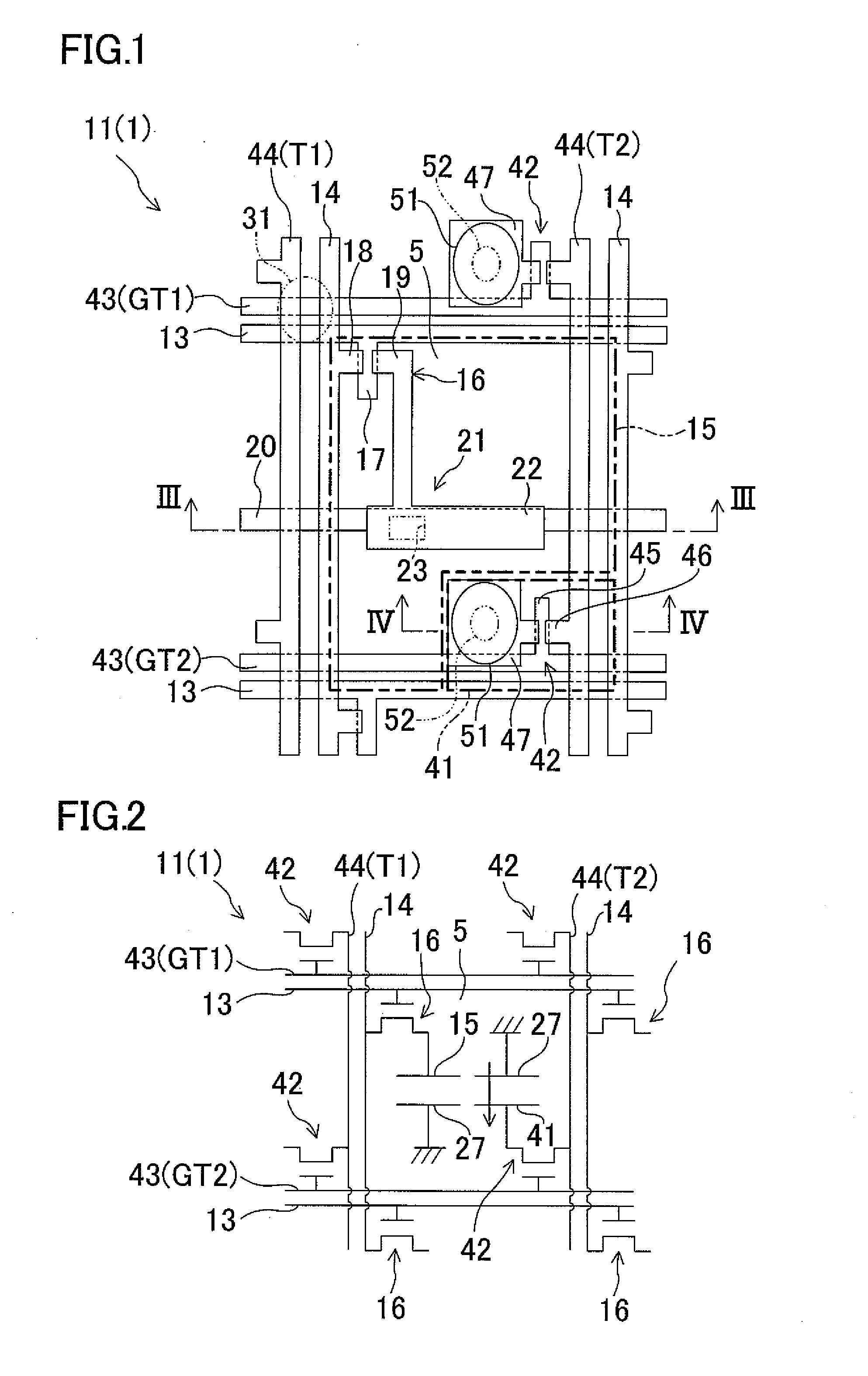
[0101]According to the second embodiment, since the touch electrode 41 and the detection element 42 are provided in each pixel 5, advantages similar to those of the first embodiment can be obtained. Moreover, since the first detection lines 43 serve also as the gate lines 13, the number of lines is reduced, whereby the aperture ratio of the pixels 5 can be increased.
Third Embodiment
[0102]FIGS. 8-9 show a third embodiment of the present invention.
[0103]FIG. 8 is an enlarged plan view of a pixel of an LCD according to the third embodiment. FIG. 9 is a circuit diagram showing a circuit configuration corresponding to FIG. 8.
[0104]In the first embodiment, the first detection lines 43 and the second detection lines 44 are connected to the detection elements 42 separately and independently of the gate lines 13 and the source lines 14 which are connected to the TFTs 16 for display, whereas in the third embodiment, the second detection lines 44 serve also as th...
third embodiment
Advantages of Third Embodiment
[0107]According to the third embodiment, since the touch electrode 41 and the detection element 42 are provided in each pixel 5, advantages similar to those of the first embodiment can be obtained. Moreover, since the second detection lines 44 serve also as the source lines 14, the number of lines is reduced, whereby the aperture ratio of the pixels 5 can be increased.
Fourth Embodiment
[0108]FIGS. 10-11 show a fourth embodiment of the present invention.
[0109]FIG. 10 is an enlarged plan view of a pixel of an LCD according to the fourth embodiment. FIG. 11 is a circuit diagram showing a circuit configuration corresponding to FIG. 10.
[0110]In the first embodiment, the touch electrodes 41 are provided separately and independently of the pixel electrodes 15, whereas in the fourth embodiment, the pixel electrodes 15 serve also as the touch electrodes 41.
[0111]That is, as shown in FIGS. 10-11, in the detection element 42 of the fourth embodiment, a drain portio...
PUM
 Abstract
Description
Claims
Application Information