LED package and method for fabricating the same

a technology of light-emitting diodes and led packages, which is applied in the direction of semiconductor/solid-state device manufacturing, electrical equipment, semiconductor devices, etc., can solve the problems of cumbersome and complicated fabrication process of led packages, difficult to consecutively fabricate led packages, and conventionally difficult to design and fabricate led packages with variably changing viewing angles. , to achieve the effect of reducing the cost of led packages, and reducing the cost of led

Inactive Publication Date: 2011-05-12
SEOUL SEMICONDUCTOR
View PDF16 Cites 27 Cited by
  • Summary
  • Abstract
  • Description
  • Claims
  • Application Information

AI Technical Summary

Benefits of technology

[0020]According to an embodiment of the present invention, a control range of a light viewing angle of an LED package is enlarged, and the LED package can be easily designed to have the desired light viewing angle. Further, it is possible to solve various problems which may be caused by a shape of an encapsulation member, such as a hot spot phenomenon, in which a contact portion between a light guide plate and the encapsulation member of the LED package is excessively bright when the LED package is used as a backlight, or the degradation of the light emitting efficiency caused by the concave shape of the encapsulation member. Further, according to an embodiment of the present invention, since the encapsulation member and the housing are formed by a transfer molding process, a molding equipment may be used as it is while a mold may be replaced with another to form both the encapsulation member and the housing, which is more economical than the prior art. Furthermore, unlike the prior art in which the encapsulation member is separately formed in a dotting manner, only one mold having a plurality of spaces for forming an encapsulation member is used, and the liquefied resin is filled in the spaces at a time and then is rapidly cured according to one embodiment of the present invention. Thus, a plurality of LED packages can be quickly fabricated, thereby largely enhancing the productivity of LED packages.

Problems solved by technology

It is conventionally difficult to design and fabricate the LED package with a viewing angle of light variably changed.
Further, since there is a large difference between the molding method of the housing and the molding method of the encapsulation member, it is difficult to consecutively fabricate the LED package and the fabrication process for the LED package is cumbersome and complicated.
On the other hand, if the amount of the liquefied resin injected into the cavity is reduced, there is generated an undesired, concave shape to thereby decrease the light emitting efficiency of the LED package.

Method used


Image

  • LED package and method for fabricating the same
  • LED package and method for fabricating the same
  • LED package and method for fabricating the same

Examples


Embodiment Construction

[0031]Hereinafter, preferred embodiments of the present invention will be described in detail with reference to the accompanying drawings. The following embodiments are provided only for illustrative purposes so that those skilled in the art can fully understand the spirit of the present invention. Therefore, the present invention is not limited to the following embodiments but may be implemented in other forms. In the drawings, the widths, lengths, thicknesses and the like of elements may be exaggerated for convenience of illustration. Like reference numerals indicate like elements throughout the specification and drawings.

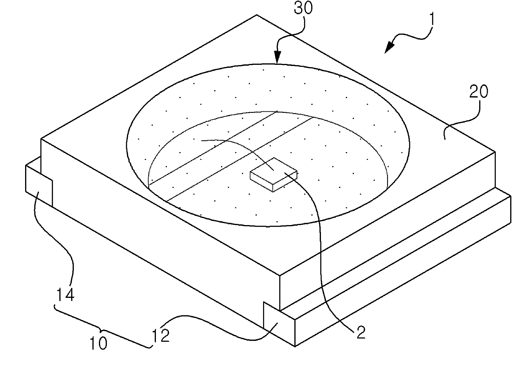
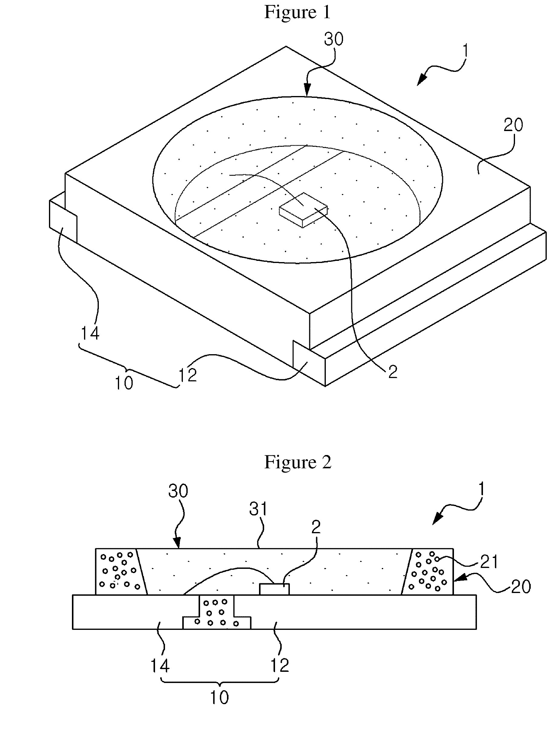
[0032]FIG. 1 is a perspective view illustrating an LED package according to an embodiment of the present invention, and FIG. 2 is a sectional view illustrating the LED package according to the embodiment of the present invention.

[0033]Referring to FIGS. 1 and 2, an LED package 1 according to this embodiment includes a lead frame 10 having a first lead terminal 12...


PUM


Abstract

An LED package is disclosed herein. The disclosed LED package comprises a base having an LED chip mounted thereon, an encapsulation member formed by a light-transmittable resin to encapsulate the LED chip, and a housing formed to expose a top portion of the encapsulation member and to encompass a side surface of the encapsulation member, wherein the encapsulation member is formed by a transfer molding process using a mold to have a predetermined shape. Further, the housing may be light-transmittable.

Description

CROSS-REFERENCE TO RELATED APPLICATIONS[0001]This application is the National Stage of International Application No. PCT / KR2008 / 007103, filed Dec. 2, 2008, and claims priority from and the benefit of Korean Patent Application No. 10-2007-0126436, filed on Dec. 6, 2007, which are both hereby incorporated by reference for all purposes as if fully set forth herein.BACKGROUND OF THE INVENTION[0002]1. Field of the Invention[0003]The present invention relates to a light emitting diode (LED) package and a method of fabricating the same, and more particularly, to an improvement of an LED package, which includes a light-transmittable encapsulation member for encapsulating an LED chip and a housing configured to surround the encapsulation member.[0004]2. Discussion of the Background[0005]An LED is a semiconductor light emitting device in which a current is supplied thereto and electrons and holes may be recombined in p-n semiconductor junctions to emit light. Conventionally, the LED is fabric...

Claims


Application Information

Patent Timeline
Patent Type & Authority Applications(United States)
IPC IPC(8): H01L33/52H01L33/48H01L33/60
CPCH01L33/486H01L33/60H01L2224/48091H01L2224/48247H01L2224/48465H01L2933/0091H01L2933/005H01L33/54H01L2924/00014H01L2924/00H01L33/62H01L33/642H01L33/641H01L33/647
Inventor LEE, CHUNG HOONKIM, YOON HEEPARK, BYUNG YEOLKIM, BANG HYUNSEO, EUN JUNGKWON, HYOUK WON
Owner SEOUL SEMICONDUCTOR
Why Eureka
Try Eureka