

Hybrid Package Construction With Wire Bond And Through Silicon Vias
a technology of wire bonding and silicon vias, applied in the field of integrated circuits, can solve the problems of large ic area, low interconnect density of wire bonding interconnects, and large size of contact pads required
- Summary
- Abstract
- Description
- Claims
- Application Information
AI Technical Summary
Problems solved by technology
Method used
Image

Examples
Embodiment Construction
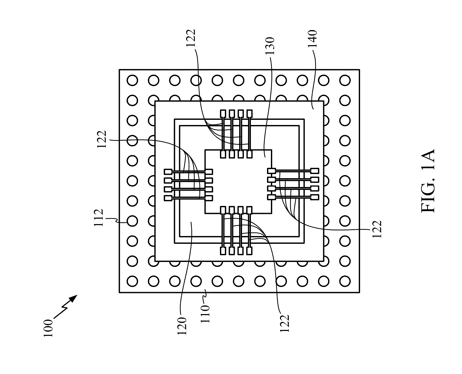
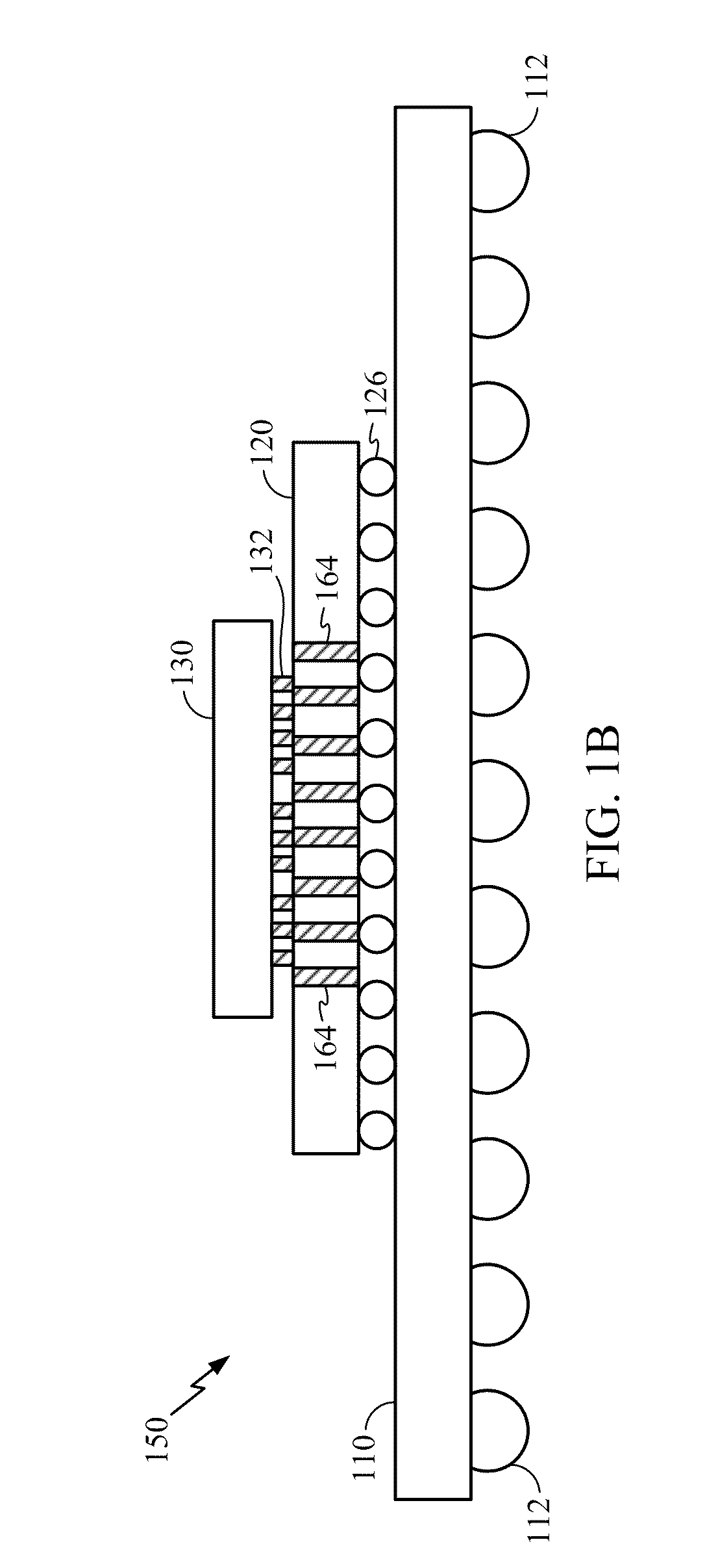
[0020]FIG. 1A is a top-down view of a conventional stacked IC having wire bond interconnects. A conventional stacked IC 100 includes a packaging substrate 110 having a packaging connection 112 such as bumps of a ball grid array (BGA). A first die 120 is coupled to the packaging substrate 110. A second die 130 is stacked on the first die 120. Communication between the second die 130 and the packaging substrate 110 is enabled through wire bonds 122. The wire bonds 122 are enclosed in a bond shell 140 for protection during later semiconductor assembly.
[0021]The bond shell 140 encompasses a larger area on the packaging substrate 110 than the first die 120. Thus, the size of the stacked IC 100 is based, in part, on the bond shell 140. Reductions in size of the first die 120 alone may not reduce the size of the stacked IC 100.
[0022]According to another configuration, microbumps may be used in place of the wire bonds 122 between the first die 120 and the packaging substrate 110. FIG. 1B is...
PUM
 Abstract
Description
Claims
Application Information