Fabrication of Nanovoid-Imbedded Bismuth Telluride with low dimensional system

a technology of nanovoids and bismuth telluride, which is applied in the direction of rigid airships, transportation and packaging, aircraft, etc., can solve the problems of poor electron mobility, lower electrical conductivity, and lower thermoelectric performance, and achieve the effect of reducing thermal conductivity and increasing electrical conductivity

Inactive Publication Date: 2011-05-19
NASA
View PDF9 Cites 9 Cited by
  • Summary
  • Abstract
  • Description
  • Claims
  • Application Information

AI Technical Summary

Benefits of technology

[0010]Another object of the present invention is to provide a fabrication method for a thermoelectric material having increased electrical conductivity.
[0013]Another object of the present invention is to provide a fabrication method for nanovoid-imbedded bismuth telluride with a high figure of merit.

Problems solved by technology

The previous studies also showed most of voids in Bi—Te film existed in an interconnected form which causes poor electron mobility, resulting in lower electrical conductivity and hence, lower thermoelectric performance.

Method used


Image

  • Fabrication of Nanovoid-Imbedded Bismuth Telluride with low dimensional system
  • Fabrication of Nanovoid-Imbedded Bismuth Telluride with low dimensional system
  • Fabrication of Nanovoid-Imbedded Bismuth Telluride with low dimensional system

Examples


Embodiment Construction

should be read together with the accompanying drawings, wherein:

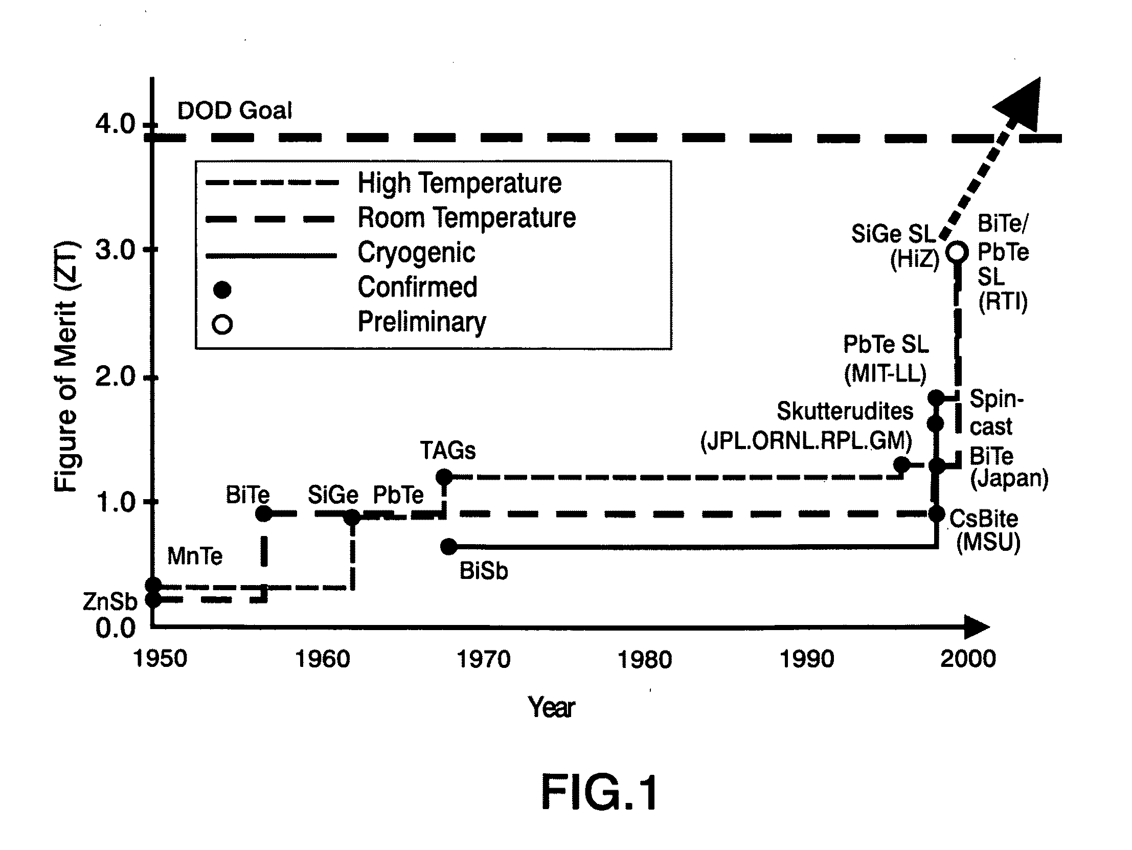
[0017]FIG. 1 is a graph depicting the History of Thermoelectric Figure of Merit (ZT);

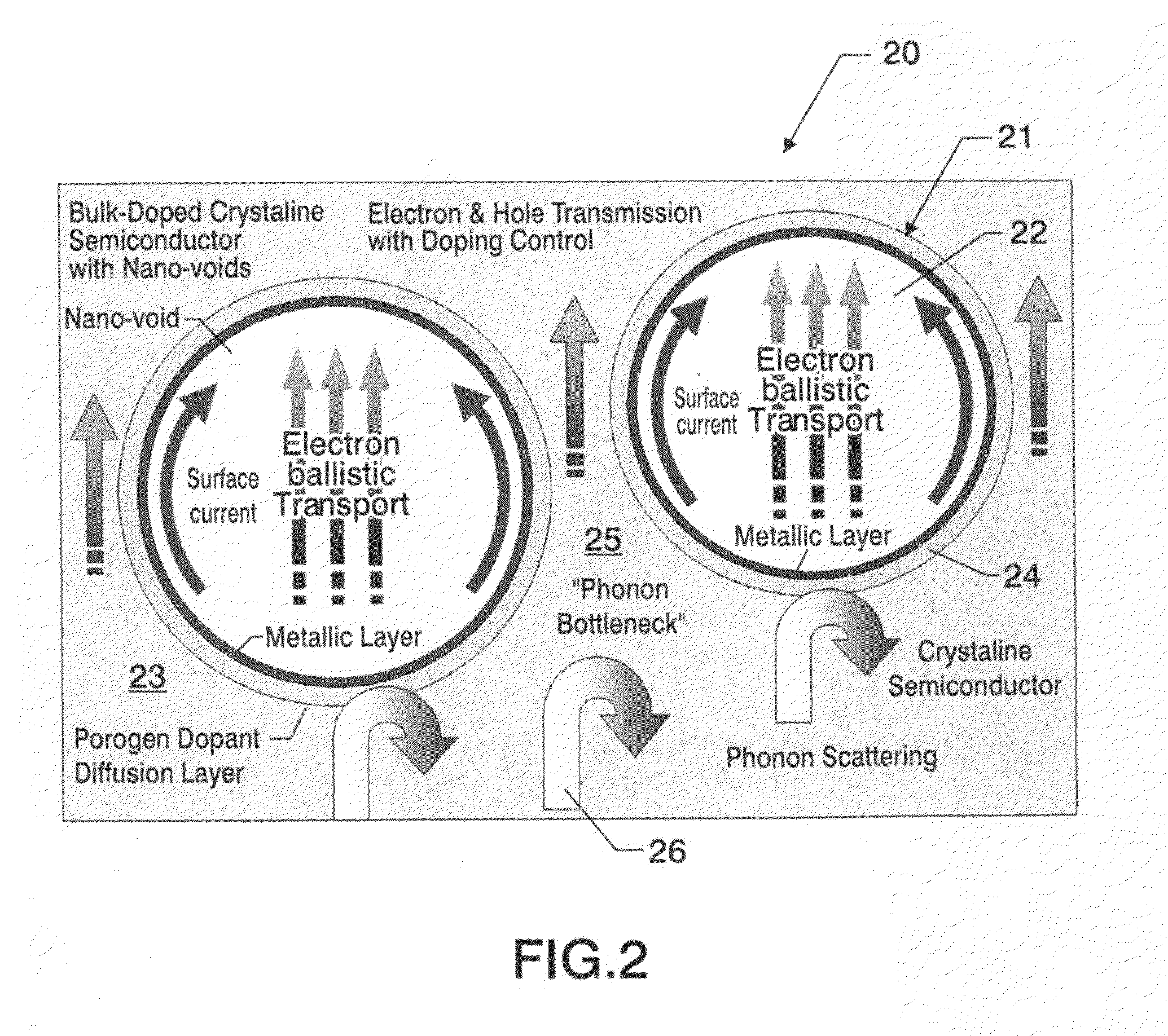
[0018]FIG. 2 is an illustration of a morphological design of an advanced thermoelectric material to enhance the ZT by increasing electrical conductivity while concurrently reducing thermal conductivity by populating nanovoids into the material, which material can be utilized in at least one embodiment of the present invention;

[0019]FIG. 3 is a graph of the figure of merit of several TE materials which could be utilized in at least one embodiment of the present invention;

[0020]FIG. 4 is a flow chart of the fabrication of a nanovoid bismuth telluride (Bi—Te) thermoelectric material that could be utilized in at least one embodiment of the present invention;

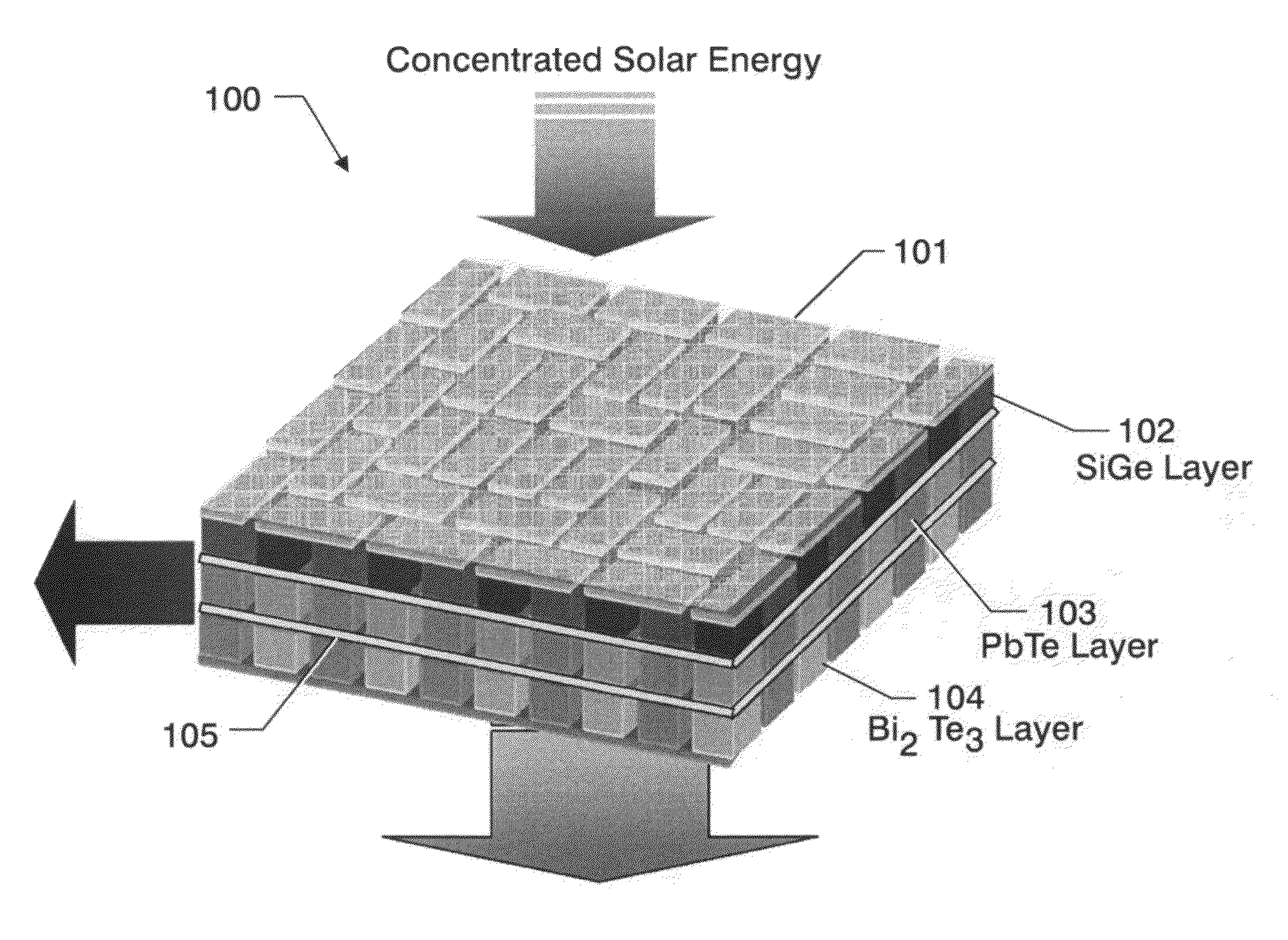
[0021]FIG. 5 is a diagram depicting a portion of the fabrication process of the Bi—Te thermoelectric material referenced in FIG. 4, i.e., the formation of low-dimensional bismuth telluri...


PUM


Abstract

A new fabrication method for nanovoids-imbedded bismuth telluride (Bi—Te) material with low dimensional (quantum-dots, quantum-wires, or quantum-wells) structure was conceived during the development of advanced thermoelectric (TE) materials. Bismuth telluride is currently the best-known candidate material for solid-state TE cooling devices because it possesses the highest TE figure of merit at room temperature. The innovative process described here allows nanometer-scale voids to be incorporated in Bi—Te material. The final nanovoid structure such as void size, size distribution, void location, etc. can be also controlled under various process conditions.

Description

CROSS-REFERENCE TO RELATED APPLICATIONS[0001]This application is a Divisional application of prior pending U.S. patent application Ser. No. 11 / 831,233 filed Jul. 31, 2007 and published Mar. 19, 2009 as U.S. 2009 / 0072078, which claims the benefit of U.S. provisional application 60 / 834,547, with a filing date of Jul. 31, 2006. The entire disclosure of the prior application is hereby incorporated by reference herein in its entirety. This invention was made in part by employees of the United States Government and may be manufactured and used by or for the Government of the United States of America for governmental purposes without the payment of any royalties thereon or therefor.STATEMENT REGARDING FEDERALLY SPONSORED RESEARCH OR DEVELOPMENT[0002]The U.S. Government has a paid-up license in this invention and the right in limited circumstances to require the patent owner to license others on reasonable terms, as provided for by the terms of Contract No. NCC-1-02043 awarded by the Nation...

Claims


Application Information

Patent Timeline
Patent Type & Authority Applications(United States)
IPC IPC(8): H01L21/20
CPCB64B1/06B64B1/20B64B1/30B64C2201/022B64C2201/042H01L35/26B64C2201/125B64C2201/127H01L35/16H01L35/22B64C2201/122B64U10/30B64U2101/35B64U50/19B64U2101/30H10N10/857H10N10/855H10N10/852B64U2101/23B64U50/31B64U2101/20
Inventor CHU, SANG-HYONCHOI, SANG HYOUKKIM, JAE-WOOPARK, YEONJOONELLIOTT, JR., JAMES R.KING, GLEN C.STOAKLEY, DIANE M.
Owner NASA
Why Eureka
Try Eureka